
Research progress in high-performance power device packaging and power cycle reliability
-
摘要:
半导体技术的进步使得功率器件面临更高的电压、功率密度和结温,这对功率器件的封装的可靠性提出了更高的要求. 如何提高和检测功率器件的可靠性已经成为功率器件发展的重要任务. 提升器件封装可靠性主要围绕优化封装结构、改进芯片贴装技术和引线键合技术3个方向研究. 功率循环作为最贴近功率器件实际工况的可靠性测试方法,其测试技术、参数监测方法和失效机理得到广泛的研究. 对功率器件封装结构、封装技术以及功率循环机理的相关研究进行了综述,总结了近年国内外的提升封装可靠性的方法,并介绍功率循环测试的原理和钎料层、键合线的失效机理,最后对于功率器件封装的未来发展趋势进行了展望.
Abstract:The progress of semiconductor technology has made power devices face higher voltage, power density and junction temperature, which puts forward higher requirements for the reliability of power device packaging. How to improve and detect the reliability of power devices has become an important task in the development of power devices. Improving packaging reliability mainly focuses on optimizing packaging structure, improving die attach technology and wire bonding technology. Power cycling, as a reliability testing method closest to the actual operating conditions of power devices, has been widely studied in terms of testing techniques, monitoring methods, and failure mechanisms. This paper provides a review of research on the packaging structure, packaging technology, power cycling mechanism of power devices and attempts to summarize the methods for improving packaging reliability at home and abroad in recent years. This review also discusses the principles of power cycling test and the failure mechanisms of solder layers and bonding wires . Finally, the future development trend of power device packaging was prospected.
-
Keywords:
- power device /
- packaging structure /
- power cycling test /
- die attach /
- wire bonding
-
0. 序言
Cu及其合金由于具有良好的导电性和导热性,被广泛用于制冷管道及设备中[1].但Cu的密度大、价格高,而Al及其合金耐蚀性十分优异,并且具有密度小、强度高、价格低等优势[2]. 在不影响使用性能的前提下,采用Cu/Al复合结构是实现轻量化和降低经济成本的十分具有前景的方法之一[3].由于Cu/Al在物理性能上的差异,传统熔化焊的方法难以实现高质量连接.尤其是在高温下,Cu,Al之间易形成脆性金属间化合物,严重降低接头的性能[4]. 因此,通常采用固相焊或钎焊的方法来获得Cu/Al焊接接头.
搅拌摩擦焊(friction stir welding,FSW)是基于摩擦焊技术的一种固相焊[5]. 焊接过程中热输入量低,可避免形成较厚的金属间化合物层,有利于提高接头的强度. Lee等人[6]采用FSW获得了Cu/Al接头,在接头中金属间化合物层较少. 然而,搅拌摩擦焊通常适用于平板类工件的焊接,难以用于管件焊接. 磁脉冲焊接(magnetic pulse welding,MPW)也属于固相焊的一种,并适用于管件的焊接[7]. 在MPW过程中,能产生金属射流以去除基体表面的氧化膜,从而实现冶金结合[8]. Raoelison等人[9]采用MPW对Cu/Al进行焊接,结果表明,在合适的工艺参数下可以有效焊接Cu/Al. Xu等人[10]采用热-力耦合欧拉模型分析了MPW的界面特性和界面温度变化. Pourabbas等人[11]采用MPW连接不同的铝合金,在合适的碰撞角度和放电能量下可获得高质量的接头. 然而,由于磁脉冲焊接过程中Cu/Al仍为直接相连的方式,无法避免脆性金属间化合物层的形成[12]. 此外,MPW接头存在孔洞和微裂纹等缺陷.
钎焊因具有生产效率高、工艺适应性好和成本低等优点被广泛应用于异种材料的焊接[13].但Cu/Al钎焊时需采用钎剂去除铝表面致密的氧化膜[14],容易导致接头产生气孔和电化学腐蚀.因此,Cu/Al无钎剂钎焊已成为研究热点.Xiao等人[15]采用超声波辅助钎焊Cu/Al接头,发现在超声振动的辅助下,接头具有良好的冶金结合.Wei等人[16]采用瞬态液相结合工艺焊接Cu/Al接头,结果发现Mg的加入可以与Al2O3反应从而分解去除氧化膜.Shi等人[17]采用半固态Zn-Al钎料钎焊铝合金及其复合材料,研究了铝表面氧化膜的去除机理和半固态钎料的变形行为.
结合磁脉冲焊接和半固态钎焊的特点,提出了一种电磁成形、半固态成形与钎焊复合的无钎剂钎焊新工艺−磁脉冲辅助半固态钎焊[18].利用电磁力驱动外管高速冲击半固态钎料,通过钎料中固相颗粒的挤压和剪切作用,使基体氧化膜破碎并清除.但前期研究发现[19],在接头搭接区域中部,会出现界面连接缺陷.受Fan等人[20]采用随形集磁器电磁成形制备Cu/Al双层金属管的启发,分析导致界面连接缺陷可能的原因是等内径集磁器的电磁力分布使搭接区域的管件变形与钎料剪切流动不协调,从而影响去膜效果及界面连接质量的均匀性.鉴于此,文中将通过改变集磁器结构,分析其钎焊过程中管件的变形行为及钎料的剪切流变行为,考察集磁器结构对接头界面连接质量、微观组织及性能的影响.
1. 试验及模拟方法
1.1 磁脉冲辅助半固态钎焊工艺原理
图1为磁脉冲辅助半固态钎焊工艺原理,分为装夹成形和钎焊成形两步工序.首先,电磁力驱动外管缩径变形并与内管贴合,如图1a所示.由于碰撞速度以及碰撞角度均未达到磁脉冲焊接所需的条件,此过程仅仅是将内、外管进行机械连接,防止后续加热时半固态钎料从底部流出.然后,将管件待焊接区域移动至集磁器工作区域,如图1b所示.对脉冲电容再次充电,同时通过感应加热线圈对内管进行加热.钎料达到所需的半固态温度后,脉冲电容再次放电进行钎焊成形.外管在电磁力的作用下高速冲击半固态钎料,使其高速剪切流动,管壁氧化膜受到钎料内部固相颗粒的挤压剪切作用从而破碎清除,如图2所示.
![]() 图 1 磁脉冲辅助半固态钎焊工艺原理Figure 1. Schematic of magnetic pulse assisted semi-solid brazing process. (a) clamping forming for the first discharge process; (b) brazing forming for the secondary discharge process
图 1 磁脉冲辅助半固态钎焊工艺原理Figure 1. Schematic of magnetic pulse assisted semi-solid brazing process. (a) clamping forming for the first discharge process; (b) brazing forming for the secondary discharge process1.2 试验方法及集磁器形状设计
有关研究结果表明[20],随形集磁器的电磁力分布能使外管与内管产生渐进式地碰撞,将其借鉴到磁脉冲辅助半固态钎焊时,可使外管对钎料的挤压由搭接区域底部至端部依次进行,使钎料剪切流动更充分,去膜效果更均匀,有利于提高整个搭接区域的界面连接质量. 为了便于加工,将集磁器简化为图3所示的形状,轮廓与装夹成形后外管的外形基本相似.
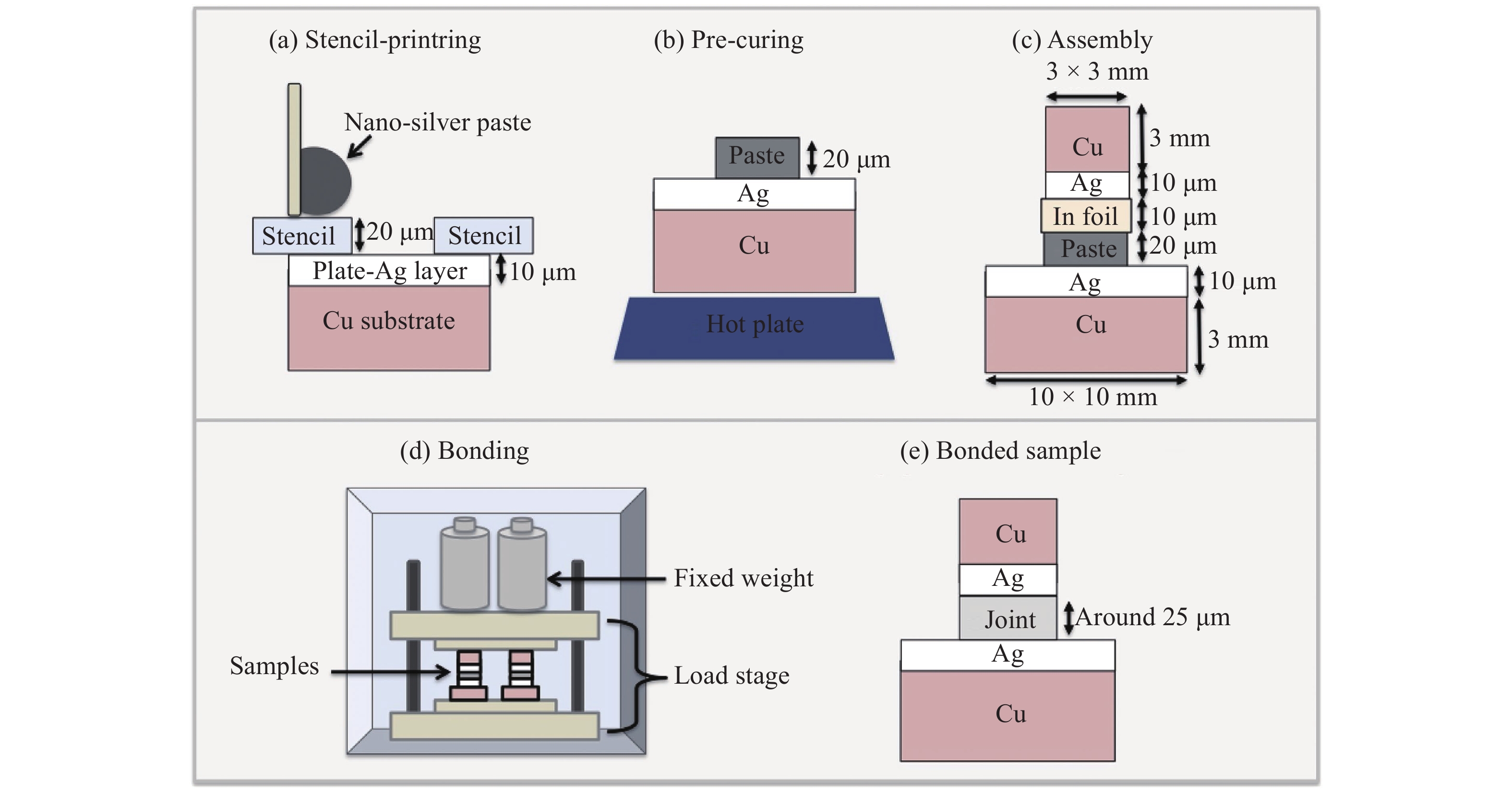
![]() 图 3 集磁器几何尺寸 (mm)Figure 3. Geometric dimensions of field shapers. (a) constant diameter field shaper; (b) cone angle field shaper
图 3 集磁器几何尺寸 (mm)Figure 3. Geometric dimensions of field shapers. (a) constant diameter field shaper; (b) cone angle field shaper磁脉冲辅助半固态钎焊的试验装置如图4所示,主要包括电磁成形机、成形线圈、集磁器、加热线圈、工件以及各种夹具.装夹成形的放电电压为7 kV,钎焊成形的放电电压为4 kV.钎焊试验中外管、内管以及钎料所采用的材料分别为1060 Al,T2 Cu和Zn-15Al合金,各材料的化学成分如表1所示. Al管外径19 mm,壁厚1 mm;Cu管外径15 mm,壁厚1.5 mm;钎料厚度为400 μm.根据课题组前期研究结果[21],将钎焊温度设为410 ℃.钎焊前,用SiC砂纸将材料表面打磨干净,并使用无水乙醇进行超声清洗5 min.
钎焊完成后,对Cu/Al接头沿纵向进行剖分,通过JXA-8230型电子探针显微分析仪(electron probe microanalyzer,EPMA)进行显微组织分析.对搭接区域沿轴向截取3个环状试样,通过万能试验机进行抗剪强度测试,以3个试样的平均抗剪强度作为Cu/Al钎焊接头的抗剪强度.
表 1 铜管、铝管及钎料化学成分(质量分数,%)Table 1. Chemical compositions of Cu tube, Al tube and solder材料 Al Zn Cu Fe Ag Si Mg Mn Ni P Pb T2 Cu — 0.003 7 余量 0.004 2 0.051 — — — 0.003 8 0.003 9 0.003 2 1060 Al 余量 0.25 0.15 0.7 — 0.4 0.8 0.15 — — — Zn-15Al 14.95 余量 0.521 0.012 — 0.031 0.01 — — — 0.002 1.3 数值模拟方法
通过有限元仿真软件LS-DYNA对磁脉冲辅助半固态钎焊过程中涉及的电磁场-结构场-流场耦合进行模拟分析.电磁场与结构场通过顺序耦合的方式进行求解,同时,通过罚刚度法对结构场及流场进行耦合,从而实现电磁场-结构场-流场的耦合.
由于外管在410 ℃下进行高速变形,因此采用Johnson-Cook本构模型以考虑应变速率敏感性、应变硬化以及温度软化效应.
$$ \sigma = (A+ B{\varepsilon _{\rm{p}}}^n)(1 + C{\rm{ln}}{\varepsilon ^*})(1 - {T^{*m}}) $$ (1) 式中:σ为流动应力;
$ {\varepsilon _{\rm{p}}} $ 为等效塑性应变;$ {\varepsilon ^*} = $ $ \varepsilon _{\rm{p}}^*/\varepsilon _0^* $ ,其中$ \varepsilon ^* $ 为无量纲应变率,$\varepsilon _{\rm{p}}^* $ 为应变率,$ \varepsilon _0^* $ 为参考应变率;${{ T}^*} = $ $ (T - {T_{\rm{r}}})/({T_{{\rm{melt}}}} - {T_{\rm{r}}})$ 为同系温度,$ {T_{{\rm{melt}}}} $ 为材料熔点,$ {T_{\rm{r}}} $ 为参考温度;A,B,n,C和m为试验所需确定的参数,如表2所示.线圈、集磁器视为刚体(几乎不变形),采用刚体材料模型;钎料及空气视为流体,采用Null材料模型,Null材料模型为LS-DYNA中一种常用的流体材料模型.表 2 1060 Al的Johnson-Cook本构模型参数Table 2. Johnson-Cook constitutive model parameters of 1060 Al屈服强度
A/MPa应变硬化模量 B/MPa 应变硬化
指数 n应变率硬化
系数 C热软化
指数m120 200 0.3 0.01 1 图5为有限元模型.线圈、集磁器、外管定义为导体,计算得到感应电流的趋肤深度为0.94 mm,小于外管壁厚,因此将钎料和内管视为绝缘体.所有部件均采用六面体单元进行网格划分,为了提高计算精度,变形区域采用较高的网格密度.
2. 结果分析及讨论
2.1 模拟结果
图6为采用等内径集磁器和带锥角集磁器时外管电流密度分布.采用等内径集磁器时,外管的电流密度分布如图6a所示.由于集磁器的端部效应,外管端部电流密度最大.而采用带锥角集磁器时,外管的电流密度集中在搭接区域底部,并且沿底部至端部呈梯度分布,如图6b所示. 这是由于外管端部与带锥角集磁器之间的距离增加所导致.
![]() 图 6 外管电流密度云图Figure 6. Current density diagram of outer tube. (a) constant diameter field shaper; (b) cone angle field shaper
图 6 外管电流密度云图Figure 6. Current density diagram of outer tube. (a) constant diameter field shaper; (b) cone angle field shaper图7为采用等内径集磁器和带锥角集磁器时外管洛伦兹力的分布情况.采用等内径集磁器情况下,由于外管端部具有最大的电流密度,因此洛伦兹力最大,如图7a所示.对于带锥角集磁器,最大洛伦兹力出现在搭接区域的底部附近,如图7b所示.
![]() 图 7 外管洛伦兹力矢量图Figure 7. Lorentz force vector diagram of outer tube. (a) constant diameter field shaper; (b) cone angle field shaper
图 7 外管洛伦兹力矢量图Figure 7. Lorentz force vector diagram of outer tube. (a) constant diameter field shaper; (b) cone angle field shaper外管在洛伦兹力的作用下以高应变速率缩径变形并与半固态钎料发生碰撞,在这种冲击作用下,钎料产生高速剪切流动.图8和图9分别为采用等内径集磁器和带锥角集磁器时钎料不同时刻的流动速度分布.在等内径集磁器情况下,由于外管底部与钎料距离最近,最先发生碰撞;另一方面,又由于外管端部洛伦兹力最大,首先发生变形并与钎料碰撞,因此钎料的剪切流动最先出现在端部及底部区域.而端部及底部的钎料沿轴向向两侧流动,阻碍了中部钎料的剪切流动,因此流速最低.可以发现,这种外管的变形模式对搭接区域内钎料的均匀剪切流动是不利的.采用带锥角集磁器时,外管由底部至端部依次与半固态钎料进行碰撞,因此钎料也从底部至端部依次产生剪切流动.
![]() 图 8 采用等内径集磁器时钎料剪切流动速度Figure 8. Shear flow velocity of solder with constant diameter field shaper. (a) t = 33 μs; (b) t = 35 μs; (c) t = 45 μs; (d) t = 60 μs; (e) t = 80 μs
图 8 采用等内径集磁器时钎料剪切流动速度Figure 8. Shear flow velocity of solder with constant diameter field shaper. (a) t = 33 μs; (b) t = 35 μs; (c) t = 45 μs; (d) t = 60 μs; (e) t = 80 μs![]() 图 9 采用带锥角集磁器时钎料剪切流动速度Figure 9. Shear flow velocity of solder with cone angle field shaper. (a) t = 33 μs; (b) t = 35 μs; (c) t = 45 μs; (d) t = 60 μs; (e) t = 80 μs
图 9 采用带锥角集磁器时钎料剪切流动速度Figure 9. Shear flow velocity of solder with cone angle field shaper. (a) t = 33 μs; (b) t = 35 μs; (c) t = 45 μs; (d) t = 60 μs; (e) t = 80 μs钎料剪切应力的大小决定了基体氧化膜能否有效去除,图10为不同位置处钎料的最大剪切应力.由图10可知,采用带锥角集磁器后,搭接区域中部钎料所受剪切应力幅值相对提高,分布更趋均匀,有利于去除该区域的氧化膜,保证界面有效结合.
2.2 试验验证
分别采用等内径集磁器和带锥角集磁器对Cu/Al管进行了磁脉冲辅助半固态钎焊试验. Cu/Al钎焊接头如图11所示,在外管的冲击作用下,部分半固态钎料被挤出.
图12为采用两种集磁器时钎焊接头中部区域的显微组织.从图12可以看到,最明显的变化是钎缝区的晶粒形状、尺寸和Cu侧界面的形貌.钎缝区主要由深灰色颗粒和颗粒周围的亮白色相组成.在等内径集磁器情况下,晶粒呈玫瑰状且较为粗大.对于带锥角集磁器,晶粒更加细小并且接近球形;晶粒尺寸由38.12 μm减小到22.18 μm,形状因子由0.67增大到0.87.这是由于在带锥角集磁器条件下,钎料所受的剪切应力更大,剪切流变速率更高,钎料的剪切流动更充分、更均匀,从而使晶粒得到更为充分、更均匀地剪切细化.由表3可知,图中深灰色颗粒为α-Al,亮白色相为Zn-Al共晶相.
表 3 图12中所标记点的EDS结果Table 3. EDS results of points marked in Fig. 12位置 Al Cu Zn O 可能的相 A 31.99 19.56 25.84 22.61 氧化物 B 82.28 — 17.72 — α-Al C 15.58 6.44 77.98 — α-Al + Zn-Al共晶 D 83.28 0.78 15.94 — α-Al E 79.16 0.44 20.40 — α-Al F 19.20 46.93 33.87 — 扩散层 G 18.59 35.33 46.08 — 扩散层 H 51.88 19.62 28.50 — α-Al + Zn-Al共晶 I 3.92 22.79 73.29 — CuZn5 J 77.80 1.67 20.54 — α-Al K 26.92 5.49 67.59 — α-Al + Zn-Al共晶 ![]() 图 12 Cu/Al钎焊接头显微组织Figure 12. Microstructure of Cu/Al brazing joint. (a) interface of Cu side with constant diameter field shaper; (b) brazed seam with constant diameter field shaper; (c) interface of Al side with constant diameter field shaper; (d) interface of Cu side with cone angle field shaper; (e) brazed seam with cone angle field shaper; (f) interface of Al side with cone angle field shaper
图 12 Cu/Al钎焊接头显微组织Figure 12. Microstructure of Cu/Al brazing joint. (a) interface of Cu side with constant diameter field shaper; (b) brazed seam with constant diameter field shaper; (c) interface of Al side with constant diameter field shaper; (d) interface of Cu side with cone angle field shaper; (e) brazed seam with cone angle field shaper; (f) interface of Al side with cone angle field shaper对于Cu侧界面,在等内径集磁器条件下,发现了不连续的扩散层,缺陷处(点A)的EDS结果显示,O元素原子分数为22.61%,表明界面处仍存在氧化物,氧化膜去除不充分,从而影响了界面的冶金结合.而在带锥角集磁器条件下,Cu侧界面扩散层连续,对应的EDS结果(点F,G)显示,界面处不存在氧化物,表明氧化膜去除充分,实现了良好的冶金结合.此外,网状的CuZn5相附着在扩散层上,并向钎缝区生长.Ji等人[22]的研究表明,这种结构有利于提高界面连接的可靠性.对于Al侧界面,在等内径集磁器和带锥角集磁器情况下均形成了连续扩散层,对应的EDS结果(点D,E)显示,氧化膜去除充分,实现了良好冶金结合.
出现上述界面连接结果的原因:内管(Cu管)没有径向变形,其表面氧化膜的去除完全靠钎料的冲刷作用,当钎料剪切应力幅值不够大时,氧化膜不能充分去除,从而导致界面存在连接缺陷;而外管(Al管)在钎焊过程中会径向高速挤压钎料,氧化膜的去除不仅依靠钎料的轴向冲刷,其与钎料的径向高速撞击也会发挥作用,故即使在等内径集磁器条件下,径向撞击及轴向剪切的综合作用已能完全去除外管表面的氧化膜,因此,两种集磁器条件下,Al侧界面均能实现良好的冶金结合.
剪切试验结果表明,在其它焊接工艺参数相同的条件下,采用等内径集磁器所获得的钎焊接头抗剪强度为46 MPa,而采用带锥角集磁器时,抗剪强度为58 MPa,提高了26%.这是因为在带锥角集磁器条件下,钎料与基体界面的冶金结合得到了改善,纤缝组织进一步细化.此外,近球状晶粒可以降低应力集中[23].在这些因素的综合作用下,钎焊接头的抗剪强度得到了提高.
文中仅针对两种特定的集磁器(等内径和带锥角),讨论其磁脉冲辅助半固态钎焊过程中管件的变形行为和钎料的剪切流变行为,阐明了集磁器结构变化对界面连接质量、焊缝组织及接头性能产生影响的原因.后续研究中,需系统考察集磁器结构参数对接头连接质量、组织性能的影响规律,并以界面连接质量和接头性能为目标,对集磁器结构参数进行优化,并最终为该新工艺的推广应用提供集磁器优化设计的依据与方法.
3. 结论
(1) 对管件磁脉冲辅助半固态钎焊工艺,等内径集磁器由于其电磁力分布不能满足无钎剂钎焊对管件变形与钎料剪切流变的协调性需求,导致搭接区域内去膜效果存在差异,在去膜不充分的局部区域,易产生界面连接缺陷.
(2) 简化的随形集磁器结构(带锥角集磁器)能够更好地满足磁脉冲辅助半固态钎焊对管件变形与钎料剪切流变的协调性需求,钎料剪切流变速率及去膜效果相对更为均匀,避免界面连接缺陷并细化搭接区域中部的纤缝组织,有效地提高界面连接质量并改善钎焊接头组织性能.
-
![]()
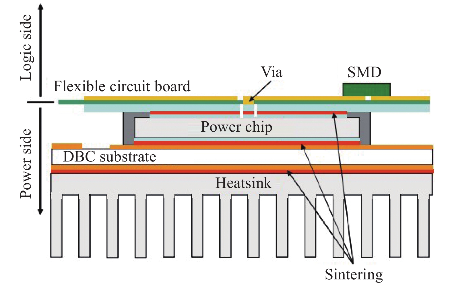
图 2 采用PCB板取代键合线的封装结构示意图[5]
Figure 2. Sectional view of packaging structure using PCB instead of bonding wire
![]()
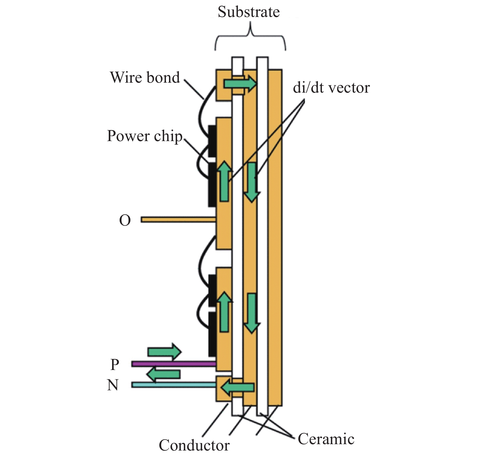
图 6 三导体双陶瓷基板结构示意图[12]
Figure 6. Sectional view of triple-conductor double-ceramic layered substrate
![]()
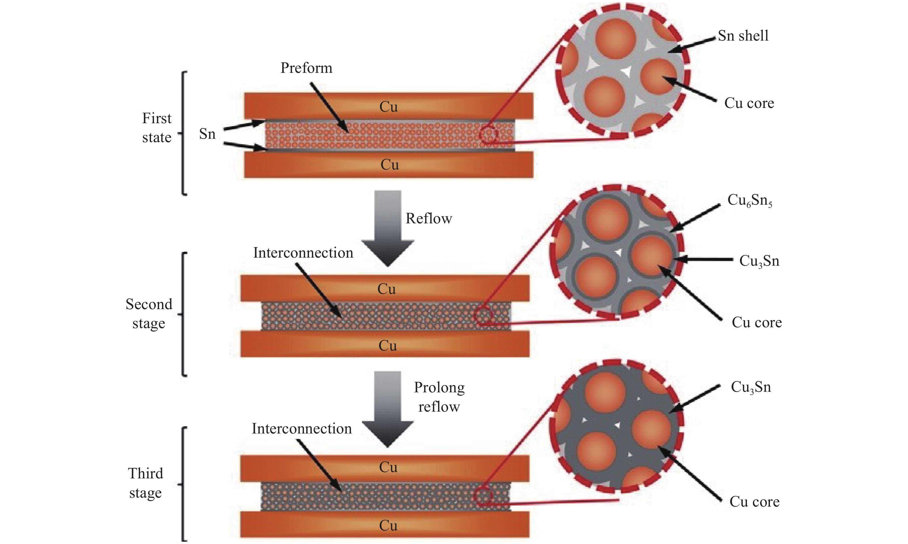
图 8 基于Cu@Sn粒子制备的高温剪切样品的结合工艺示意图[21]
Figure 8. Schematic diagram of the bonding process for the high-temperature shearing sample based on a preform fabricated with Cu@Sn particles
![]()
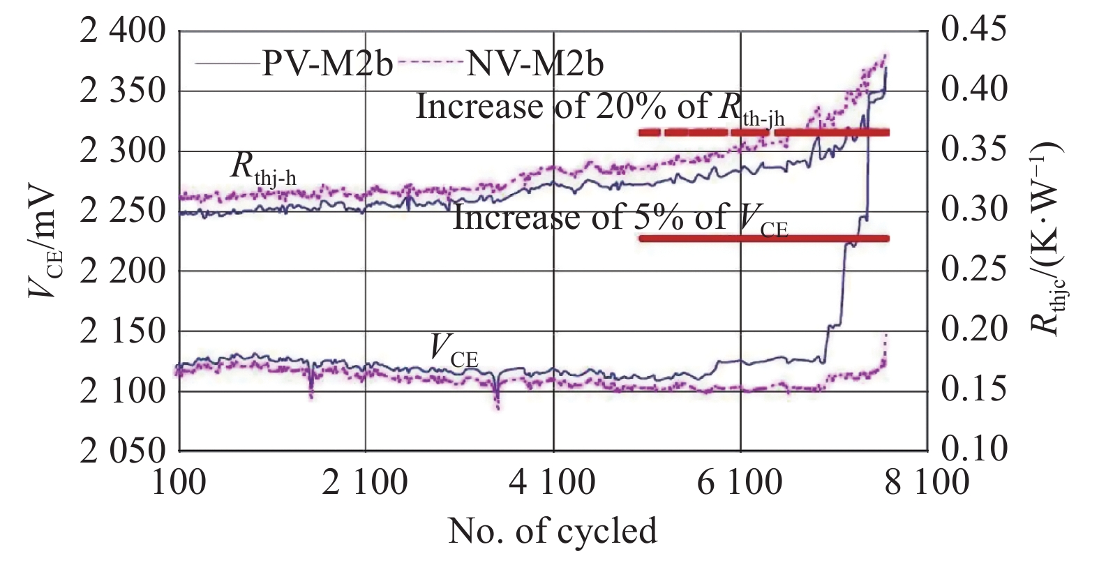
图 11 ECONOPACK电源模块APC测试期间VCE和Rthjc的演变[41]
Figure 11. Evolution of VCE and Rthjc during APC testing of ECONOPACK power module
![]()
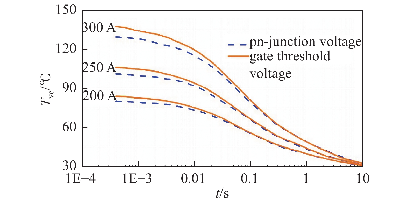
图 12 650 V IGBT器件两种方法测量结温过程的对比[45]
Figure 12. Comparison of two methods for measuring junction temperature in 650 V IGBT devices
![]()
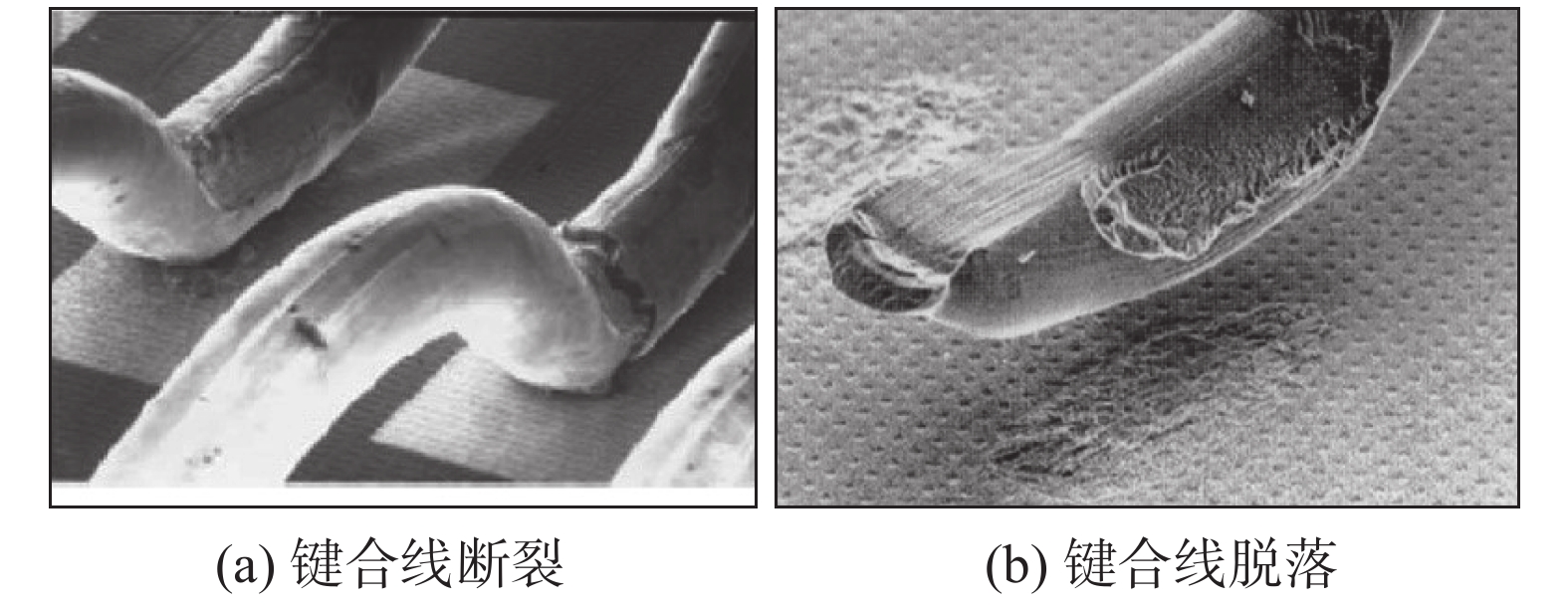
图 13 键合线根部断裂和脱落的微观形貌[55]
Figure 13. Microscopic morphology of fracture and detachment at the root of the bonding line. (a) fracture; (b) detachment
-
[1] Yoder M N. Wide bandgap semiconductor materials and devices[J]. IEEE Transactions on Electron Devices, 1996, 43(10): 1633 − 1636. doi: 10.1109/16.536807
[2] 蔡蔚, 杨茂通, 刘洋, 等. SiC 功率模块封装技术及展望[J]. 汽车工程, 2022, 44(4): 638 − 648. Cai Wei, Yang Maotong, Liu Yang, et al. SiC power module packaging technologies and prospects[J]. Automotive Engineering, 2022, 44(4): 638 − 648.
[3] Hou F, Wang W, Cao L, et al. Review of packaging schemes for power module[J]. IEEE Journal of Emerging and Selected Topics in Power Electronics, 2019, 8(1): 223 − 238.
[4] Dimarino C, Boroyevich D, Burgos R, et al. Design and development of a high-density, high-speed 10 kV SiC mosfets module[C]//2017 19th European Conference on Power Electronics and Applications (EPE'17 ECCE Europe). IEEE, 2017.
[5] Ikeda Y, Iizuka Y, Hinata Y, et al. Investigation on wirebond-less power module structure with high-density packaging and high reliability [C]//IEEE, 2011.
[6] Stabach J, Cole Z, O'neal C, et al. A high performance power package for wide bandgap semiconductors using novel wire bondless power interconnections[J]. International Symposium on Microelectronics, 2015(1): 000353 − 000358. doi: 10.4071/isom-2015-WP16
[7] Stockmeier T, Beckedahl P, Göbl C, et al. SKiN: double side sintering technology for new packages [C]//2011 IEEE 23rd International Symposium on Power Semiconductor Devices and ICs. IEEE, 2011.
[8] Zhu N, Mantooth H A, Xu D, et al. A solution to press-pack packaging of SiC mosfets[J]. IEEE Transactions on Industrial Electronics, 2017, 64(10): 8224 − 8234. doi: 10.1109/TIE.2017.2686365
[9] Liang Z. Integrated double sided cooling packaging of planar SiC power modules [C]//2015 IEEE Energy Conversion Congress and Exposition (ECCE). IEEE, 2015: 4907 − 4912.
[10] Boteler L M, Miner S M, Hinojosa M. Co-designed high voltage module [C]//2018 17th IEEE Intersociety Conference on Thermal and Thermomechanical Phenomena in Electronic Systems (ITherm). IEEE, 2018: 824 − 830.
[11] Fabian J, Hartmann S, Hamidi A. Partial discharge failure analysis of AlN substrates[J]. Microelectronics Reliability, 2004, 44: 1425 − 1430. doi: 10.1016/j.microrel.2004.07.111
[12] Tanimoto S, Matsui K. High junction temperature and low parasitic inductance power module technology for compact power conversion systems[J]. IEEE Transactions on Electron Devices, 2015, 62(2): 258 − 269. doi: 10.1109/TED.2014.2359978
[13] Chen C, Chen Y, Li Y, et al. An SiC-based half-bridge module with an improved hybrid packaging method for high power density applications[J]. IEEE Transactions on Industrial Electronics, 2017, 64(11): 8980 − 8991. doi: 10.1109/TIE.2017.2723873
[14] 杨东升, 张贺, 冯佳运, 等. 电子封装微纳连接技术及失效行为研究进展[J]. 焊接学报, 2022, 43(11): 126 − 136. doi: 10.12073/j.hjxb.20220702003 Yang Dongsheng, Zhang He, Feng Jiayun, et al. Research progress of low-temperature Cu-Cu bonding technology for advanced packaging[J]. Transactions of the China Welding Institution, 2022, 43(11): 126 − 136. doi: 10.12073/j.hjxb.20220702003
[15] 冯洪亮. Ni-Sn TLPS连接特性与动力学研究 [D]. 北京: 北京科技大学, 2018. Feng Hongliang. Study on the characteristics and kinetics of Ni-Sn TLPS bonding process[D]. Beijing: University of Science and Technology Beijing, 2018.
[16] Yamada Y, Takaku Y, Yagi Y, et al. Pb-free high temperature solder joints for power semiconductor devices[J]. Transactions of the Japan Institute of Electronics Packaging, 2009, 2(1): 79 − 84. doi: 10.5104/jiepeng.2.79
[17] Tanimoto S, Matsui K, Zushi Y, et al. Eutectic Zn-Al die attachment for higher Tj SiC power applications: Fabrication method and die shear strength reliability[J]. Journal of Microelectronics and Electronic Packaging, 2013, 10(2): 59 − 66. doi: 10.4071/imaps.373
[18] Liu H, Xue S, Tao Y, et al. Design and solderability characterization of novel Au–30Ga solder for high-temperature packaging[J]. Journal of Materials Science:Materials in Electronics, 2020, 31: 2514 − 2522. doi: 10.1007/s10854-019-02787-8
[19] 刘晗, 薛松柏, 王刘珏, 等. 金基中低温钎料的研究现状与展望[J]. 材料导报, 2019, 33(19): 3189 − 3195. doi: 10.11896/cldb.18090164 Liu Han, Xue Songbai, Wang Liuyu, et al. Research status and prospect of Au-based medium-low temperature filler metals[J]. Materials Reports, 2019, 33(19): 3189 − 3195. doi: 10.11896/cldb.18090164
[20] Li Z, Li M, Xiao Y, et al. Ultrarapid formation of homogeneous Cu6Sn5 and Cu3Sn intermetallic compound joints at room temperature using ultrasonic waves[J]. Ultrasonics Sonochemistry, 2014, 21(3): 924 − 929. doi: 10.1016/j.ultsonch.2013.09.020
[21] Hu T, Chen H, Li M. Die attach materials with high remelting temperatures created by bonding Cu@ Sn microparticles at lower temperatures[J]. Materials & Design, 2016, 108: 383 − 390.
[22] 邹贵生, 闫剑锋, 刘磊, 等. 纳米金属颗粒膏合成及其低温烧结连接的电子封装应用研究进展[J]. 机械制造文摘(焊接分册), 2013(1): 12 − 16. Zou Guisheng, Yan Jianfeng, Liu Lei, et al. Development of the synthesis of metal nanoparticle paste[J]. Welding Digest of Machinery Manufacturing, 2013(1): 12 − 16.
[23] 贾强, 邹贵生, 张宏强, 等. 纳米颗粒材料作中间层的烧结连接及其封装应用研究进展[J]. 机械工程学报, 2022, 58(2): 2 − 16. Jia Qiang, Zou Guisheng, Zhang Hongqiang, et al. Research progress in sintering-bonding with nanoparticle materials as interlayer and its packaging application[J]. Journal of Mechanical Engineering, 2022, 58(2): 2 − 16.
[24] Yang C, Yang S, Liu X, et al. Enhancement of nano-silver chip attachment by using transient liquid phase reaction with indium[J]. Journal of Alloys and Compounds, 2018, 762: 586 − 597. doi: 10.1016/j.jallcom.2018.05.254
[25] Alayli N, Schoenstein F, Girard A, et al. Spark plasma sintering constrained process parameters of sintered silver paste for connection in power electronic modules: Microstructure, mechanical and thermal properties[J]. Materials Chemistry and Physics, 2014, 148(1-2): 125 − 133. doi: 10.1016/j.matchemphys.2014.07.021
[26] 迟聪聪, 夏亮, 王曌, 等. 丙三醇-水二元溶剂法抗氧化纳米铜的制备[J]. 包装工程, 2020, 41(13): 131 − 138. doi: 10.19554/j.cnki.1001-3563.2020.13.018 Chi Congcong, Xia Liang, Wang Zhao, et al. Preparation of antioxidant copper nanoparticles in glycerol-water binary solvent system[J]. Packaging Engineering, 2020, 41(13): 131 − 138. doi: 10.19554/j.cnki.1001-3563.2020.13.018
[27] Ji H, Zhou J, Liang M, et al. Ultra-low temperature sintering of Cu@ Ag core-shell nanoparticle paste by ultrasonic in air for high-temperature power device packaging[J]. Ultrasonics Sonochemistry, 2018, 41: 375 − 381. doi: 10.1016/j.ultsonch.2017.10.003
[28] 徐瑜, 戴东方, 杨仁彬, 等. 甲酸处理的纳米铜无压烧结性能及. 高温老化研究[J]. 重庆大学学报, 2023(10): 1 − 10. Xu Yu, Dai Dongfang, Yang Renbin, et al. Research on pressureless sintering performance and high temperature aging of formic acid-treated nano-copper[J]. Journal of Chongqing University, 2023(10): 1 − 10.
[29] Zhou H, Zhang Y, Cao J, et al. Research progress on bonding wire for microelectronic packaging[J]. Micromachines, 2023, 14(2): 432. doi: 10.3390/mi14020432
[30] Ling J M, Xu T, Chen R, et al. Cu and Al-Cu composite-material interconnects for power devices [C]//62nd IEEE Electronic Components and Technology Conference (ECTC). San Diego, CA, 2012: 1905 − 1911.
[31] Zhao J, Qin F, An T, et al. Electro-thermal and thermal-mechanical FE analysis of IGBT module with different bonding wire shape [C]//2017 18th International Conference on Electronic Packaging Technology (ICEPT). IEEE, 2017: 548 − 551.
[32] Celnikier Y, Dupont L, Herve E, et al. Optimization of wire connections design for power electronics[J]. Microelectronics Reliability, 2011, 51(9-11): 1892 − 1897. doi: 10.1016/j.microrel.2011.06.058
[33] European Center for Power Electronics. Qualification of power modules for use in power electronics converter units (PCUs) in motor vehicles: AQG 324 [S]. Nuremberg, Germany: ECPE Working Group, 2018.
[34] 陈杰, 邓二平, 张一鸣, 等. 功率循环试验中开通时间对高压大功率IGBT模块失效模式的影响及机理分析[J]. 中国电机工程学报, 2020, 40(23): 7710 − 7721. doi: 10.13334/J.0258-8013.PCSEE.200667 Chen Jie, Deng Erping, Zhang Yiming, et al. Influence and mechanism analysis of load pulse duration on failure mode of high power IGBT module under power cycling condition[J]. Proceedings of the CSEE, 2020, 40(23): 7710 − 7721. doi: 10.13334/J.0258-8013.PCSEE.200667
[35] Tounsi M, Oukaour A, Tala-Ighil B, et al. Characterization of high-voltage IGBT module degradations under PWM power cycling test at high ambient temperature[J]. Microelectronics Reliability, 2010, 50(9-11): 1810 − 1814. doi: 10.1016/j.microrel.2010.07.059
[36] 谢露红, 赵雨山, 常桂钦, 等. DC功率循环与PWM功率循环的差异对比分析[J]. 半导体技术, 2021, 46(10): 808 − 818. doi: 10.13290/j.cnki.bdtjs.2021.10.012 Xie Luhong, Zhao Yushan, Chang Guiqin, et al. Comparison and analysis of the difference between dc power cycling and PWM power cycling[J]. Semiconductor Technology, 2021, 46(10): 808 − 818. doi: 10.13290/j.cnki.bdtjs.2021.10.012
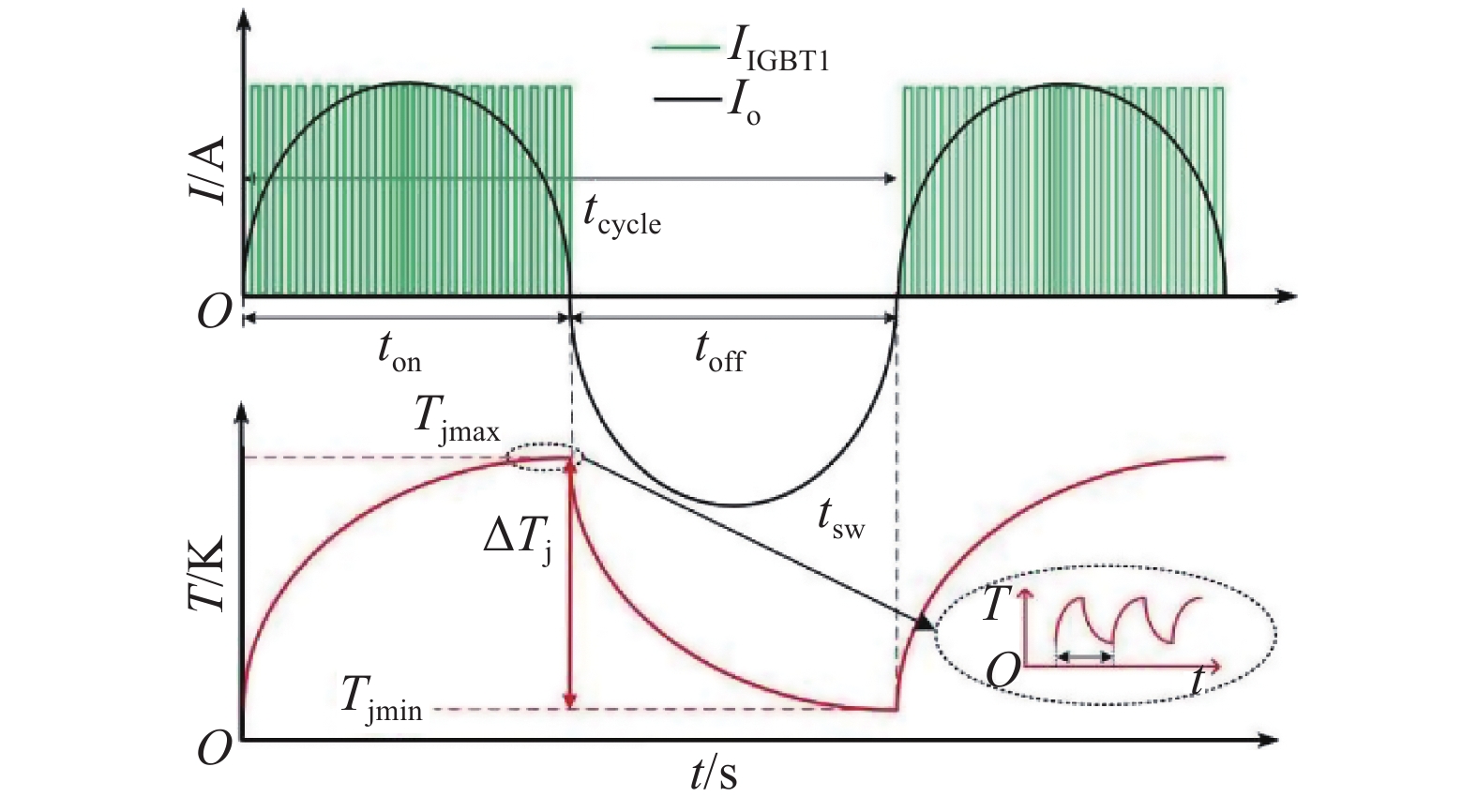
[37] 邓二平, 严雨行, 陈杰, 等. 功率器件功率循环测试技术的挑战与分析[J]. 中国电机工程学报, 2023, 43(13): 5132 − 5151. Deng Erping, Yan Yuxing, Chen Jie, et al. Power cycling test technologies for power semiconductor devices-challenges and analysis[J]. Proceedings of the CSEE, 2023, 43(13): 5132 − 5151.
[38] Herold C, Franke J, Bhojani R, et al. Requirements in power cycling for precise lifetime estimation[J]. Microelectronics Reliability, 2016, 58: 82 − 89. doi: 10.1016/j.microrel.2015.12.035
[39] Herold C, Beier M, Lutz J, et al. Improving the accuracy of junction temperature measurement with the square-root-t method [C]//19th International Workshop on Thermal Investigations of ICs and Systems (THERMINIC). IEEE. 2013: 92-94.
[40] 邓二平, 陈杰, 赵雨山, 等. IGBT封装形式对结温测量精度的影响[J]. 半导体技术, 2018, 43(12): 956 − 963. doi: 10.13290/j.cnki.bdtjs.2018.12.013 Deng Erping, Chen Jie, Zhao Yushan, et al. Influence of IGBT package types on the accuracy of junction temperature measurement[J]. Semiconductor Technology, 2018, 43(12): 956 − 963. doi: 10.13290/j.cnki.bdtjs.2018.12.013
[41] Amro D-I R. Power cycling capability of advanced packaging and interconnection technologies at high temperature swings [D]. Chemnitz: Technische Universitat Chemnitz, 2006.
[42] 陈杰, 邓二平, 赵雨山, 等. 高压大功率器件结温在线测量方法综述[J]. 中国电机工程学报, 2019, 39(22): 6677 − 6688. Chen Jie, Deng Erping, Zhao Yushan, et al. Review of on-line junction temperature measurement methods of high voltage power electronics[J]. Proceedings of the CSEE, 2019, 39(22): 6677 − 6688.
[43] Wei H, Zhiwen C. Review on failure analysis of interconnections in power devices[J]. China Welding, 2022, 31(1): 6 − 14.
[44] Schmidt R, Scheuermann U. Using the chip as a temperature sensor-The influence of steep lateral temperature gradients on the Vce (T)-measurement[J]. Epe Journal, 2011, 21(2): 5 − 11. doi: 10.1080/09398368.2011.11463790
[45] Zeng G, Cao H, Chen W, et al. Difference in device temperature determination using pn-junction forward voltage and gate threshold voltage[J]. IEEE Transactions on Power Electronics, 2018, 34(3): 2781 − 2793.
[46] 陈杰. 功率循环试验中芯片温度分布特性的测量方法研究 [D]. 北京: 华北电力大学(北京) , 2022. Chen Jie, Research on measurement method of temperature distribution characteristics on the chip in power cycling test[D]. Beijing: North China Electric Power University, 2022.
[47] 石巍. 大功率IGBT模块健康状态信息提取方法研究及加速老化试验平台研制 [D]. 杭州: 浙江大学, 2018. Shi Wei. Research on state-of-health exteacton method of high power IGBT modules and design of the accelarated aging testpPlatform system[D]. Hangzhou: Zhejiang University, 2018.
[48] 孙鹏菊, 王海波, 龚灿, 等. 短路电流作为绝缘栅双极型晶体管模块键合线老化特征量的机理研究[J]. 中国电机工程学报, 2019, 39(16): 4876 − 4883. doi: 10.13334/j.0258-8013.pcsee.181566 Sun Pengju, Wang Haibo, Gong Can, et al. Mechanism research of short-circuit current as bond wire ageing indicator of insulated gate bipolar transistor module[J]. Proceedings of the CSEE, 2019, 39(16): 4876 − 4883. doi: 10.13334/j.0258-8013.pcsee.181566
[49] Wang K, Zhou L, Sun P, et al. Monitoring bond wire defects of IGBT module using module transconductance[J]. IEEE Journal of Emerging and Selected Topics in Power Electronics, 2021, 9(2): 2201 − 2211. doi: 10.1109/JESTPE.2020.2973348
[50] 曾杰, 檀浩浩, 杨方, 等. IGBT模块焊层的被动热循环可靠性分析[J]. 焊接学报, 2023, 44(7): 123 − 128. doi: 10.12073/j.hjxb.20220517002 Zeng Jie, Tan Haohao, Yang Fang, et al. Reliability analysis of solder layer of IGBT module under passive thermal cycling[J]. Transactions of the China Welding Institution, 2023, 44(7): 123 − 128. doi: 10.12073/j.hjxb.20220517002
[51] Li H, An R, Wang C, et al. Effect of Cu grain size on the voiding propensity at the interface of SnAgCu/Cu solder joints[J]. Materials Letters, 2015, 144: 97 − 99. doi: 10.1016/j.matlet.2015.01.013
[52] 孙海峰, 杨舒曼. 焊料层空洞对绝缘栅双极型晶体管(IGBT)模块温度分布的影响[J]. 科学技术与工程, 2018, 18(32): 189 − 194. doi: 10.3969/j.issn.1671-1815.2018.32.029 Sun Haifeng, Yang Shuman. Influence of solder void on temperature distribution of insulated gate bipolar transistor ( IGBT) module[J]. Science Technology and Engineering, 2018, 18(32): 189 − 194. doi: 10.3969/j.issn.1671-1815.2018.32.029
[53] 江南, 陈民铀, 徐盛友, 等. 计及裂纹损伤的IGBT模块热疲劳失效分析[J]. 浙江大学学报(工学版), 2017, 51(4): 825 − 833. doi: 10.3785/j.issn.1008-973X.2017.04.025 Jiang Nan, Chen Minyou, Xu Shengyou, et al. Thermal fatigue of IGBT module considering crack damage[J]. Journal of Zhejiang University(Engineering Science), 2017, 51(4): 825 − 833. doi: 10.3785/j.issn.1008-973X.2017.04.025
[54] 郭秋亚. IGBT模块的焊料层疲劳失效机理研究 [D]. 天津: 天津理工大学 , 2020. Guo Qiuya. Study on fatigue failure mechanism of IGBT module's solder layer[D]. Tianjin: Tianjin University of Technology, 2020.
[55] 王学梅, 张波, 吴海平. 基于失效物理的功率器件疲劳失效机理[J]. 电工技术学报, 2019, 34(4): 717 − 727. doi: 10.19595/j.cnki.1000-6753.tces.171414 Wang Xuemei, Zhang Bo, Wu Haiping. A review of fatigue mechanism of power devices based on physics-of-failure[J]. Transactions of the China Electrotechnical Society, 2019, 34(4): 717 − 727. doi: 10.19595/j.cnki.1000-6753.tces.171414
[56] Czerny B, Lederer M, Nagl B, et al. Thermo-mechanical analysis of bonding wires in IGBT modules under operating conditions[J]. Microelectronics Reliability, 2012, 52(9-10): 2353 − 2357. doi: 10.1016/j.microrel.2012.06.081
[57] Dornic N, Ibrahim A, Khatir Z, et al. Analysis of the aging mechanism occurring at the bond-wire contact of IGBT power devices during power cycling[J]. Microelectronics Reliability, 2020, 114: 113873. doi: 10.1016/j.microrel.2020.113873
-
期刊类型引用(0)
其他类型引用(1)

 下载:
下载:


计量
- 文章访问数: 449
- HTML全文浏览量: 285
- PDF下载量: 199
- 被引次数: 1
