
Research progress of low-temperature Cu-Cu bonding technology for advanced packaging
-
摘要: Cu-Cu低温键合技术是先进封装的核心技术,相较于目前主流应用的Sn基软钎焊工艺,其互连节距更窄、导电导热能力更强、可靠性更优. 文中对应用于先进封装领域的Cu-Cu低温键合技术进行了综述,首先从工艺流程、连接机理、性能表征等方面较系统地总结了热压工艺、混合键合工艺实现Cu-Cu低温键合的研究进展与存在问题,进一步地阐述了新型纳米材料烧结工艺在实现低温连接、降低工艺要求方面的优越性,概述了纳米线、纳米多孔骨架、纳米颗粒初步实现可图形化的Cu-Cu低温键合基本原理. 结果表明,基于纳米材料烧结连接的基本原理,继续开发出宽工艺冗余、窄节距图形化、优良互连性能的Cu-Cu低温键合技术是未来先进封装的重要发展方向之一.Abstract: Low-temperature Cu-Cu bonding technology is the core technology for advanced packaging. Compared with the mainstream Sn-based soldering process, it can achieve finer pitch, higher electrical and thermal conductivity. In this paper, low-temperature Cu-Cu bonding technology for advanced packaging is reviewed. The research progress of low-temperature Cu-Cu bonding realized by thermal compression bonding and hybrid bonding is systematically summarized from the aspects of process flow, bonding mechanism and performance characterization. The advantages of the newly-developed nanomaterial sintering process in reducing bonding temperature and process requirements are further expounded. Mechanism of patterned nanowires, nano-porous frameworks and nanoparticles for low-temperature bonding are summarized. Low-temperature Cu-Cu bonding technology for advanced packaging are forecast.
-
Keywords:
- advanced packaging /
- hybrid bonding /
- Cu-Cu bonding /
- fine pitch /
- sintering
-
0. 序言
工业燃气轮机与航空发动机热端部件因服役条件恶劣[1-2],易产生表面与结构损伤[3-5],如对其直接进行报废换新会造成严重的资源浪费[6]. 激光熔覆技术作为一种高效、柔性、绿色的直接成形技术[7-8],相比于电弧堆焊、喷涂等成形修复技术,具有热影响区域小[9]、材料应用面广[10]、熔覆层结合力强[11]等优点,在修复失效热端部件中具有明显优势.
当前研究中通常采用工艺稳定[12-13]的送粉式激光熔覆实现热端部件的失效修复. Onuike等人[14]研究了修复区域轮廓对修复成形质量的影响,结果表明,因粉末与激光在修复表面过渡平滑,修复区梯形轮廓比距形轮廓更容易实现低缺陷修复.卢朋辉等人[15]研究了激光工艺对K418高温合金修复区开裂行为的影响,研究发现,随着扫描速度与激光功率的降低,熔池快速凝固产生的热应力减小,修复区产生的微裂纹数量降低.卞宏友等人[16]使用GH536粉末修复了GH738高温合金试样,结果表明,Mo,Cr元素引起的固溶强化作用,使修复区的拉伸性能、硬度高于GH536 锻件.
相比于送粉式激光熔覆,送丝式激光熔覆在材料利用率[17]、熔覆层表面形貌[18]、熔覆层成形质量[19]等方面具有优势.李凯斌等人[20]研究了不同激光工艺对送丝激光熔覆层表面形貌的影响,结果表明,当激光能量密度为100 J/mm2、熔丝率为39.44 × 10−6 g/J时,熔覆过程稳定,熔覆层表面光滑饱满. Abioye等人[21]研究了激光功率、送丝速度、扫描速度对熔覆层稀释率的影响规律,研究发现,熔覆层稀释率与激光功率、扫描速度呈正相关,与送丝速度呈负相关,通过工艺参数调控可获得稀释率良好、表面形貌光滑的熔覆层. Demir等人[22]使用送丝式激光熔覆增材制造了纵横比高达20的薄壁构件,结果表明,金属丝材的利用效率接近100%,熔覆区域显微硬度沿增材方向分布均匀.
送粉与送丝方式下高温合金激光增材修复质量存在不同,为指导修复应用中的工艺选择,文中开展了送粉式与送丝式激光修复Inconcel 718高温合金V形槽对比试验研究.结合数值模拟、高速摄像、修复试样分析等方法,对比送粉与送丝方式下激光修复过程中V形槽的温度场、熔池表面轮廓、修复区宏观形貌与微观组织差异,分析了因送粉与送丝方式差异而引起的激光能量吸收与传递的变化,并讨论修复区差异的形成机制. 该研究结果为高温合金激光增材修复应用中的材料输送方法选择提供参考.
1. 试验方案与数值模型建立
1.1 试验材料与方法
激光增材修复对比试验平台如图1所示,主要由激光器、高速相机、控制系统、冷却系统、送粉器与送丝器组成.试验采用送粉与送丝两种方式对V形槽进行激光修复,并通过高速相机对修复过程进行拍摄与记录.
![]() 图 1 送粉式与送丝式激光修复试验平台Figure 1. Experimental setup for laser repairing with powder feeding and wire feeding
图 1 送粉式与送丝式激光修复试验平台Figure 1. Experimental setup for laser repairing with powder feeding and wire feeding试验所用的基板、粉末、丝材材料均为Inconel 718镍基高温合金,化学成分如表1所示.基板尺寸为100 mm × 60 mm × 6 mm, V形槽槽深为1 mm,开口角度为60°.粉末粒径范围为100~150 μm,丝材直径为1 mm.试验所用激光功率为1 kW,光斑直径为2 mm,激光扫描速度为9 mm/s. 经前期试验探明,送粉试验的粉末利用率约为送丝试验的20%,因此修复试验中送粉和送丝量分别为18 g/min和3.6 g/min. 根据已知丝材直径,换算得送丝速度为9.3 mm/s.
表 1 Inconel 718镍基高温合金的化学成分(质量分数,%)Table 1. Chemical compositions of nickel-based superalloy Inconel 718Ni Cr Nb Mo Co Al Ti Si Mn C Cu Fe 50 ~ 55 17 ~ 21 4.75 ~ 5.5 2.8 ~ 3.3 ≤1 0.2 ~ 0.8 0.7 ~ 0.15 ≤0.35 ≤0.35 ≤0.08 ≤0.3 余量 试验开始前,对试板表面进行打磨抛光,去除表面氧化膜和油渍.采用DZF-6051型真空干燥箱,对金属粉末进行干燥处理1 h. 试验过程中,通过高速相机拍摄修复区内熔池外形尺寸.试验结束后,通过线切割进行取样处理,并分别采用KEYENCE VK-X1000型共聚焦显微镜、ZEISS Axio Imager2型光学显微镜和ZEISS EVO 18型扫描电子显微镜对修复区表面形貌、显微组织以及晶粒尺寸取向进行表征.
1.2 数值模型建立
在激光修复V形槽中,送粉或送丝方式的选用,将影响V形槽对激光能量的吸收. 基于COMSOL多物理场耦合软件建立数值模型,对比分析送粉与送丝条件下V形槽的温度场变化. 试验所采用激光功率密度为318 W/mm2,根据文献[23]与前期试验结果,该激光工艺无法在高温合金Inconel 718材料表面形成深蚀孔,因此可忽略激光在材料深度方向上的热输入.在模拟中,激光热源采用表面高斯热源[24-25],激光热源输入能量密度Q为
$$ Q = \frac{{2\alpha P}}{{\text{π} {r_{\rm{L}}}^2}}\exp \left[ {\frac{{ - 2{r^2}}}{{{r_{\rm{L}}}^2}}} \right] $$ (1) 式中:α为材料对激光的吸收率;P为激光功率;r为至光斑中心的距离;rL为光斑半径.
激光修复过程中发生热传导、热对流、热辐射等物理过程,传热控制表达式为
$$ \rho {C_{\rm{p}}}\frac{{\partial T}}{{\partial t}} + \nabla \cdot ( - k\nabla T) = Q + {q_{0}} $$ (2) 式中:ρ为材料的密度;Cp为材料的恒压热容;t为时间;T为温度;k为材料的导热系数;q0为热对流与热辐射能量密度.
对流换热的控制表达式为
$$ {Q_{{\rm{c}}}} = - h\left( {T - {T_0}} \right) $$ (3) 式中:h为表面对流换热系数;T0为环境温度,为293 K.
热辐射的控制表达式为
$$ {Q_{{\rm{d}}}} = - \varepsilon \sigma \left( {{T^4} - {T_0}^4} \right) $$ (4) 式中:ε为表面辐射率;σ为Stenfan-Boltzmann常数,为5.67 × 10⁻⁸ W/(m2∙K4);T0为环境温度,为293 K.
参考文献[26-28],设置基板初始温度为293 K,表面对流换热系数为100 W/(m2∙K),表面辐射率为0.3. 设置IN718高温合金材料的导热系数、密度、恒压热容等物性参数随温度变化.
数值模型采用改变表面热源施加位置的方法,模拟送粉与送丝方式下激光在V形槽内的不同辐照深度.在送粉式激光增材修复过程中,部分激光辐射能量被粉末流吸收,根据文献[29],在粉末粒径70 ~ 250 μm送粉量18 g/min的条件下粉末吸收约13%的辐射能量,剩余大部分激光能量穿过粉末流直接作用于工件表面.在模拟中设置粉末吸收后的激光能量直接作用于V形槽内壁.在送丝式激光修复V形槽过程中,熔池与丝材间形成稳定液桥过渡,绝大部分激光能量被熔池与丝材遮挡,模拟设置激光能量作用于熔池表面并通过熔池传递至V形槽内壁.为考虑激光在截面上的移入与移出过程,计算激光热源的加载时长. 激光光斑尺寸为2 mm,扫描速度为9 mm/s,激光经过截面所需时间为0.22 s,模拟设置激光能量随时间从0 ~ 0.11 s时,增加至激光能量分布最大值;并从0.11 ~ 0.22 s时,降低至0.根据送粉式与送丝式不同的传热方式,分别建立如图2所示的传热边界条件.
![]() 图 2 送粉式与送丝式激光修复模拟中的传热边界条件Figure 2. Boundary condition in simulation of laser repairing. (a) powder feeding method; (b) wire feeding method
图 2 送粉式与送丝式激光修复模拟中的传热边界条件Figure 2. Boundary condition in simulation of laser repairing. (a) powder feeding method; (b) wire feeding method2. 结果与分析
2.1 V形槽修复区温度场数值模拟
送粉式与送丝式激光修复V形槽的温度场模拟结果如图3所示.两种V形槽修复方式的温度场存在显著差别.在送粉式激光修复过程中,呈高斯分布的激光能量直接辐照至V形槽表面,修复区最高温度(2444.7 K)出现在V形槽底部;V形槽底部温度梯度集中,最大温度梯度为2.6 × 10³ K/mm.在送丝式激光修复过程中,激光能量通过熔池传递至V形槽内壁,修复区最高温度(2127.8 K)出现在V形槽两侧开口;修复区温度梯度分布较送粉式均匀,最大温度梯度为1.5 × 10³ K/mm.根据IN718高温合金熔点温度1493 K[27],绘制熔池相变轮廓线.通过几何测量,对比送粉送丝方式下V形槽熔深变化. 送粉式和送丝式熔深分别为1.58 mm和1.12 mm. 相比于送丝式,送粉式修复区熔深增大41.07%.
![]() 图 3 送粉式与送丝式激光修复V形槽温度场模拟结果Figure 3. Simulated temperature field during laser cladding. (a) temperature distribution; (b) temperature gradient distribution
图 3 送粉式与送丝式激光修复V形槽温度场模拟结果Figure 3. Simulated temperature field during laser cladding. (a) temperature distribution; (b) temperature gradient distribution2.2 熔池表面轮廓动态监测
图4为熔池表面轮廓变化情况. 图4中虚线为初始V形槽两侧轮廓,实线为熔池表面轮廓.在送粉式激光修复过程中,随着金属粉末进入V形槽底部熔池,熔池高度、宽度逐渐增加,熔池表面轮廓倾斜.在t0 + 0.2 s,t0 + 0.4 s,t0 + 0.6 s时,均能观察到金属粉末以固态及半固态形式冲击进入熔池,熔池表面轮廓不规则.而在送丝式激光修复过程中,丝材在激光热源的作用下不断熔化并填充修复V形槽,受表面张力影响,熔池轮廓水平.在t0 + 0.2 s,t0 + 0.4 s,t0 + 0.6 s时,均可发现熔化丝材通过液桥平稳流入熔池,熔池表面轮廓光滑.
![]() 图 4 送粉式与送丝式激光修复过程熔池轮廓Figure 4. Monitoring of the molten pool profile. (a) powder feeding method; (b) wire feeding method
图 4 送粉式与送丝式激光修复过程熔池轮廓Figure 4. Monitoring of the molten pool profile. (a) powder feeding method; (b) wire feeding method2.3 修复区表面形貌与显微组织
图5为送粉与送丝方式下V形槽修复区表面形貌,送粉式V形槽修复区表面粘有大量未熔粉末,表面粗糙度较大. 基于2.2节高速相机监测,粉末对熔池冲击明显,送粉式修复区的高度起伏明显,而送丝式修复区表面较光洁.送粉式和送丝式修复区表面轮廓最大高度Rz分别为165.1 μm和68.3 μm.进一步测量了图5中a,b,c区域(区域面积500 μm × 500 μm)的修复区表面平均表面粗糙度Ra.送粉式修复区和送丝式修复区Ra值分别13.5 μm和2.4 μm.相较于送粉式,送丝式修复区平均粗糙度Ra降低了82.2%.
![]() 图 5 送粉式与送丝式修复区表面形貌Figure 5. Surface morphology of the laser repaired zone with the powder feeding and wire feeding
图 5 送粉式与送丝式修复区表面形貌Figure 5. Surface morphology of the laser repaired zone with the powder feeding and wire feeding图6为激光修复区金相显微组织. 送粉式修复区底部能量集中,修复区熔合线在修复区中心明显下凹,熔深为1.6 mm. 送丝式修复区凝固过程中各方向温度梯度分布均匀,修复区熔合线呈半圆形,熔深大小为1.1 mm. 根据计算对比,送粉式修复区相比于送丝式熔深增大45.5%.
![]() 图 6 送粉式与送丝式修复区显微组织Figure 6. Microstructure of the laser repaired zone. (a) powder feeding method; (b) wire feeding method
图 6 送粉式与送丝式修复区显微组织Figure 6. Microstructure of the laser repaired zone. (a) powder feeding method; (b) wire feeding method通过分析修复区显微组织组成可以发现,送粉与送丝方式下,修复区显微组织均由长条柱状枝晶与块状转向枝晶组成,其凝固枝晶生长演变过程相似.在凝固开始时,枝晶垂直熔合线向修复区中心外延生长,随着凝固过程的推进在修复区中心发生转向.然而,因送粉与送丝方式V形槽修复区温度场不同. 在送粉方式下,修复区枝晶比送丝式更快转向.
2.4 修复区晶粒尺寸与取向
图7为送粉式与送丝式修复区晶粒尺寸分布. 在送粉与送丝方式下,修复区晶粒尺寸分布存在差异.送粉式修复区熔深较大,修复区底部受V形槽基板在深度方向上受激冷[30]作用影响显著,修复区凝固过程中熔池底部与顶部的温度梯度G、生长速度R、过冷度变化明显,晶粒尺寸随修复深度减小而逐渐增大,晶粒尺寸均匀性较差.送丝式修复区熔深较小,且修复区底部避免了激光直接辐照,激光能量通过熔池传递至修复区底部,因此基板产生的激冷作用在修复深度方向上并不明显.送丝式修复区凝固过程中温度梯度G、生长速度R、过冷度较送粉式变化较小,晶粒尺寸沿修复深度无明显变化,晶粒尺寸均匀性比送粉式好.因修复采用激光热源,输入能量密度相同,送粉式与送丝式修复区平均晶粒尺寸无明显差别,根据统计计算,送粉式与送丝式修复区平均晶粒尺寸分别为56.7 μm和58.5 μm.
![]() 图 7 送粉式与送丝式修复区晶粒尺寸Figure 7. Grain size of the laser repaired zone. (a) powder feeding method; (b) wire feeding method
图 7 送粉式与送丝式修复区晶粒尺寸Figure 7. Grain size of the laser repaired zone. (a) powder feeding method; (b) wire feeding method图8为送粉式与送丝式激光修复V形槽晶粒取向. 受高温度梯度影响,送粉式与送丝式修复区均呈现明显取向性. 根据图8b和图8d极图统计,送粉式与送丝式下修复区最大均匀分布(MUD)值分别为2.6与3.2. 送粉式与送丝式修复区整体取向无明显差别.相比于送丝式,送粉式修复区熔深较大,凝固过程中最大热流方向沿修复深度发生了明显转变,修复区中部上下区域晶粒取向差异明显,上下各局部区域内取向一致性强. 从图8a和图8c可知,送粉式修复区底部中心位置转向枝晶的择优取向为<101>,<111>,并随熔深减小,逐渐向<001>转变.与送粉式修复区不同,送丝式修复区中心位置转向枝晶择优取向为<101>,<111>,不发生<001>方向转变.
![]() 图 8 送粉式与送丝式修复区晶粒取向Figure 8. Grain orientation of the laser repaired zone. (a) IPF of powder feeding method; (b) pole figure of powder feeding method; (c) IPF of wire feeding method; (d) pole figure of wire feeding method
图 8 送粉式与送丝式修复区晶粒取向Figure 8. Grain orientation of the laser repaired zone. (a) IPF of powder feeding method; (b) pole figure of powder feeding method; (c) IPF of wire feeding method; (d) pole figure of wire feeding method3. 讨论
在送粉式与送丝式激光修复过程中,粉末/丝材对激光能量的遮挡效果不同,影响了V形槽与熔池对激光能量吸收与传递,使V形槽修复过程中温度场和熔池表面轮廓不同,导致修复区域的宏观形貌与微观组织存在差异.
送粉式与送丝式激光修复过程中,V形槽与熔池对激光能量吸收与传递关系如图9所示. 送粉式激光修复过程中,粉末对激光的遮挡作用较小[31],激光能量直接辐照至V形槽表面.首先在V形槽底部形成熔池,并随着粉末的填充逐渐增大.在熔池形成后,激光后端能量通过熔池传递至V形槽两侧表面.因前后端激光对V形槽传热方式不同,修复区熔合线中心明显向下突出.而送丝式激光修复过程中,丝材直径占V形槽总开口宽度的90%,且丝材位于V形槽中心位置,激光前端能量被丝材遮挡,丝材在激光作用下逐渐熔化与熔池间形成稳定液桥过渡[32]. 因激光能量被丝材、液桥、熔池吸收,并通过熔池传递至V形槽两侧表面.前后端激光对V形槽传热方式相同,V形槽内各方向上温度梯度大小接近,修复区熔合线为半圆形.
![]() 图 9 送粉式与送丝式激光修复中激光能量的吸收与传递Figure 9. Absorption and transfer of laser energy during laser repairing. (a) powder feeding method; (b) wire feeding method
图 9 送粉式与送丝式激光修复中激光能量的吸收与传递Figure 9. Absorption and transfer of laser energy during laser repairing. (a) powder feeding method; (b) wire feeding method送粉与送丝方式下V形槽修复区温度场不同,导致修复区域凝固晶粒尺寸与取向存在差异.送粉式激光修复过程中,修复区底部首先形成熔池,根据2.1节结果,因激光直接辐照,V形槽底部温度梯度G较大. 受基板激冷作用影响,底部修复区熔池散热条件好,过冷度、冷却速度较大,因此在修复区底部,大量晶粒形核并在短时间内相互挤压竞争生长,形成细小柱状晶与转向晶,凝固形成晶粒尺寸较小[33],中心转向晶粒择优取向为<111>,<101>.随着修复过程进行,修复区熔池不断增大,晶粒生长空间增大,并且激光持续的热输入,导致激光后端基板对熔池凝固所引起的激冷作用减小.因此随修复深度减小,固液界面前温度梯度G降低,过冷度、冷却速度减小,晶粒尺寸增大[34].因修复区熔深较大,熔池凝固过程中最大热流方向沿修复深度变化向激光扫描方向转变[35],凝固形成转向枝晶择优取向转变为<001>.送丝式激光修复过程中,修复区熔深较小,晶粒在修复深度方向上未产生明显的竞争生长,修复区底部避免了激光直接辐照,激光能量通过熔池传递至修复区底部,基板产生的激冷作用在修复深度方向上相比于送粉式修复区并不明显.修复区各处过冷度、冷却速度较送粉式变化较小,凝固形成晶粒尺寸分布均匀.受大温度梯度影响,底部柱状枝晶向熔池中心生长[36],并在顶部中心区域沿最大热流方向转向[37],择优取向为<111>,<101>,因送丝式修复区熔深较浅,转向枝晶未继续向<001>方向转变.
基于送粉式与送丝式V形槽修复区宏观形貌与微观组织的对比分析可知,送粉式激光修复区底部能量集中,熔合线中心明显向下突出,熔深较大.送粉式激光修复相比于送丝式,更容易获得底部熔合良好的修复区,对修复激光设备功率、修复激光工艺要求较低.然而较大的熔深会对修复件带来更深的热影响,并且引起修复区凝固过程中底部与顶部的温度梯度、过冷度、冷却速度相差较大,这使修复区晶粒尺寸分布与晶粒取向差异明显. 送丝式激光修复相比于送粉式,在修复区热影响深度、晶粒尺寸均匀性方面具有优势. 根据不同激光设备功率与缺陷外形,可选用送粉或送丝方式进行激光修复.当激光设备功率不足,缺陷外形深宽比较大时,选用送粉式激光修复,可以避免因缺陷底部能量不足而引起的熔合不良[38]. 当激光设备功率充足,缺陷外形深宽比较小时,选用送丝式激光修复,可以获得表面形貌良好、热影响区域小、晶粒尺寸分布均匀的凝固组织.
4. 结论
(1) 相比于送丝式,送粉式修复过程中,因粉末冲击影响,熔池轮廓不规则,修复区表面平均粗糙度增大82.2%.在送粉方式下,激光前端对V形槽底部直接辐照,V形槽底部修复区温度、温度梯度大于送丝式,修复区熔深增大45.5%.
(2) 相比于送丝式,送粉式激光修复过程中,V形槽基板对熔池的激冷作用在修复深度方向上变化显著,并且因前后端激光对V形槽传热方式不同,熔池内温度梯度G、过冷度、冷却速度(G × R)沿修复深度减小而减小,修复成形晶粒尺寸均匀性较差,修复区上下区域晶粒取向差异明显.
(3) 当激光设备功率不足,缺陷外形深宽比较大时,选用送粉式激光修复,可以避免因缺陷底部能量不足而引起的熔合不良;当情况相反时,选用送丝式激光修复,可以获得表面形貌良好,热影响区小,晶粒尺寸分布较均匀的凝固组织.
-
![]()
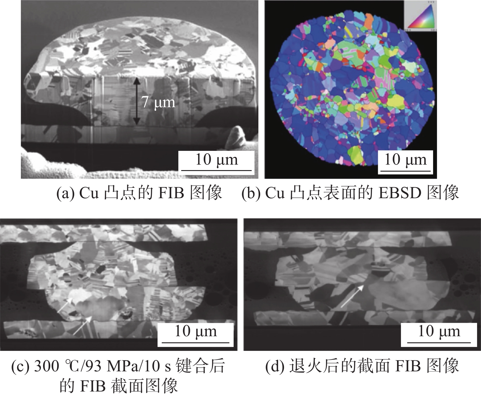
图 1 由(111) 取向的纳米孪晶Cu凸点实现Cu-Cu键合[15-17]
Figure 1. Cu-Cu bonding enabled by (111)-oriented nanotwinned Cu bumps. (a) The microbump cross-section analyzed by FIB; (b) surface orientation of an nt-Cu microbump observed by EBSD; (c) cross-sectional FIB ion-image of a Cu joint bonded at 300 ℃/93 MPa/10 s; (d) cross-sectional FIB ion-image for post-annealed sample
![]()
图 2 飞行切割[19]
Figure 2. Fly-cutting. (a) schematic illustration of fly-cutting; (b) optical images of cut Cu bumps surface
![]()
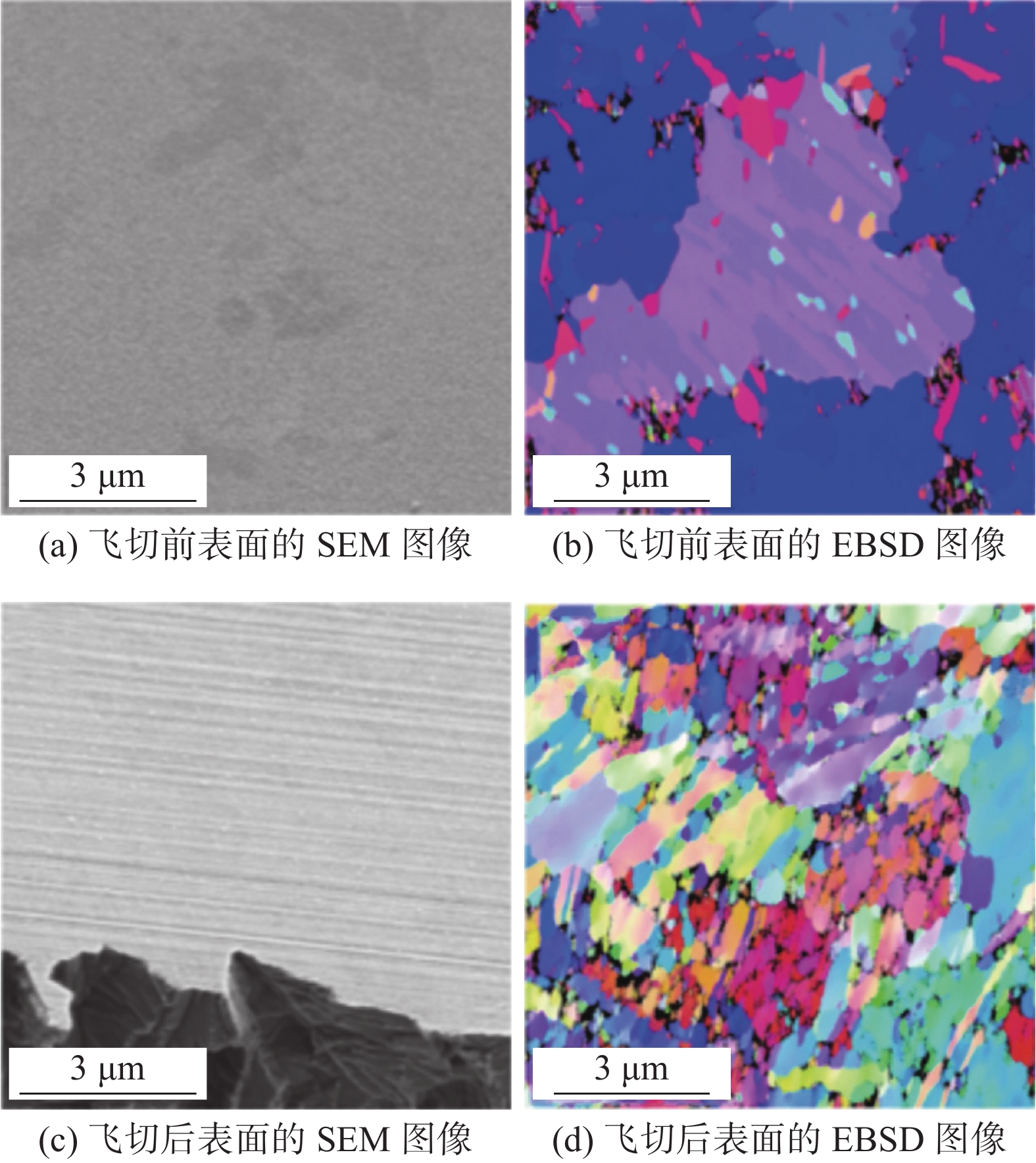
图 3 飞行切割细化表面晶粒[20]
Figure 3. Fly-cutting process introduces finer grains. (a) SEM image of initial Cu surface; (b) EBSD image of initial Cu surface; (c) SEM image of cut Cu surface; (d) EBSD image of cut Cu surface
![]()
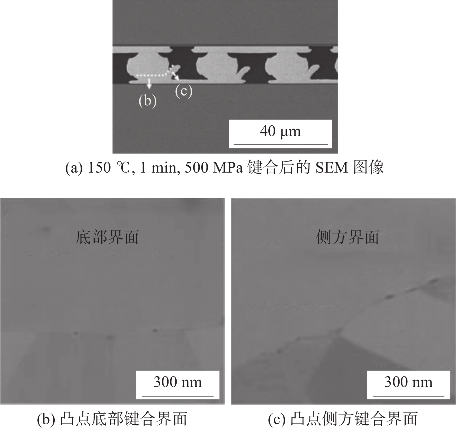
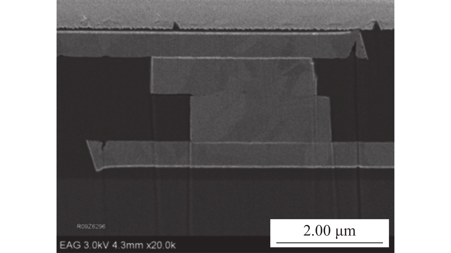
图 5 键合后的SEM图像[22]
Figure 5. SEM cross-sectional view of Cu-Cu bonding. (a) with bonding condition of 150 ℃, 1 min, 500 MPa; (b) bottom bonding interface; (c) sidewall bonding interface
![]()
![]()
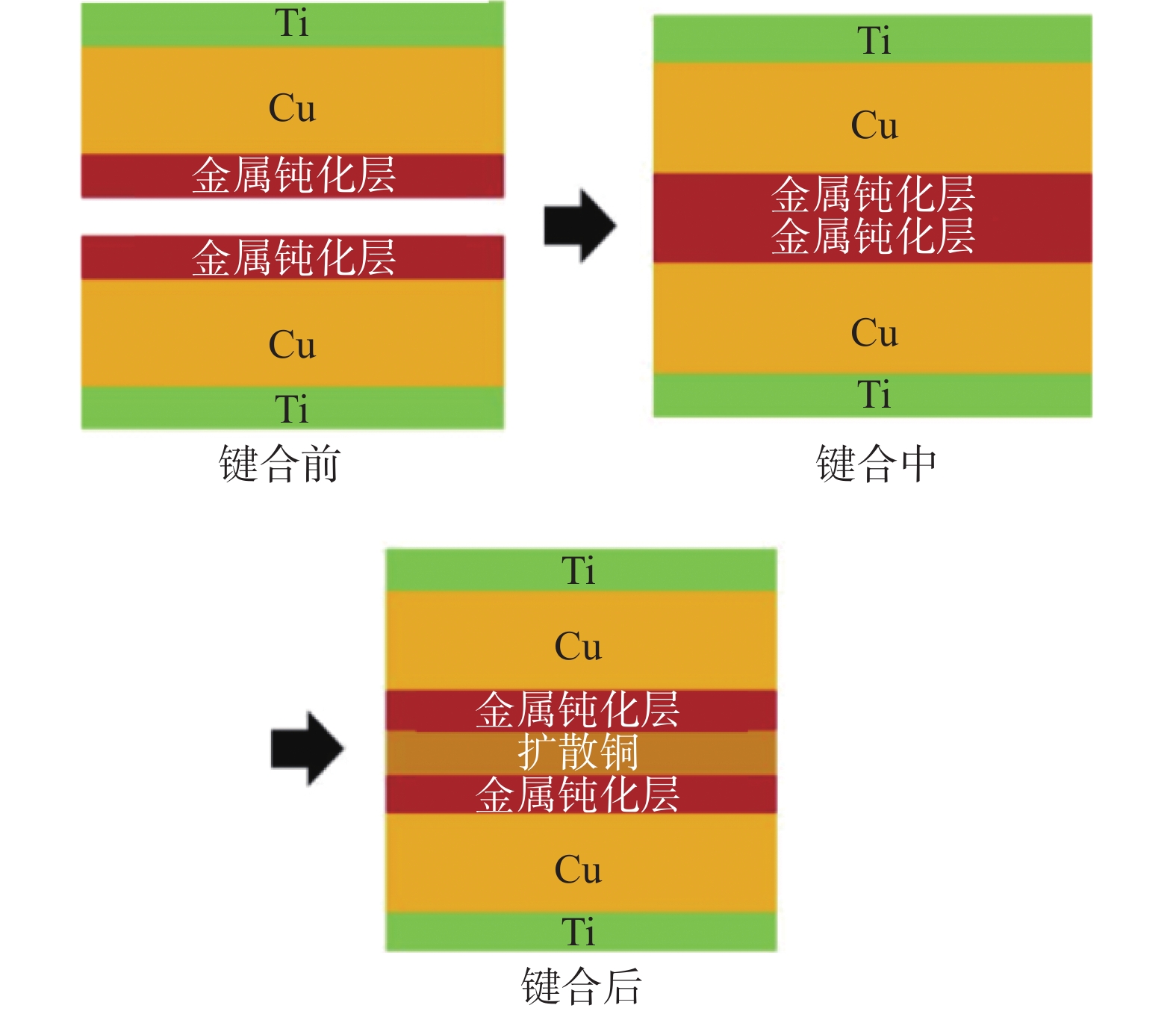
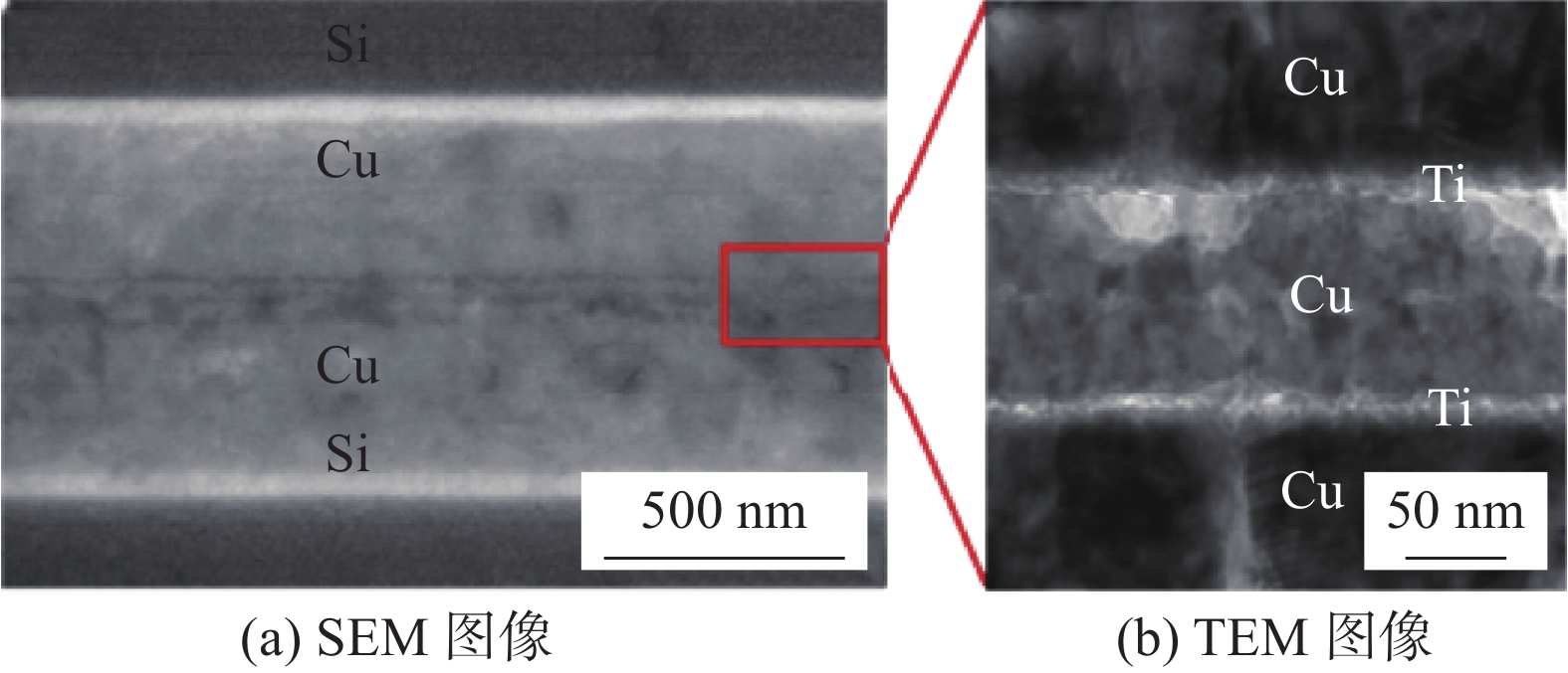
图 8 Ti作钝化层的键合结果[26]
Figure 8. Ti passivation bonded results. (a) SEM image; (b) TEM image
![]()
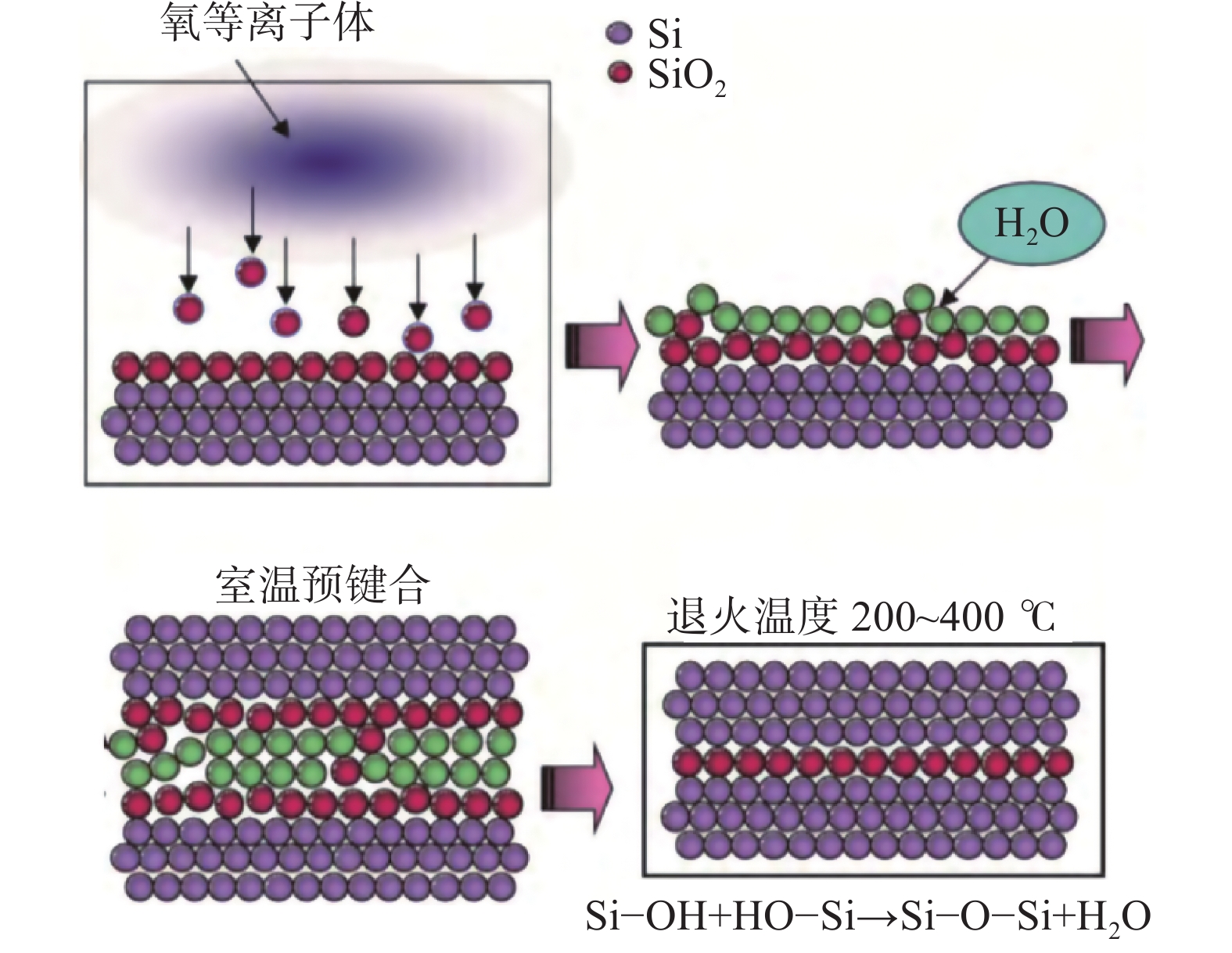
图 9 自组装分子层钝化方法的原理和工艺流程[31]
Figure 9. Schematic illustration and process flow of self-assembled monolayer method. (a) before bonding; (b) after bonding
![]()
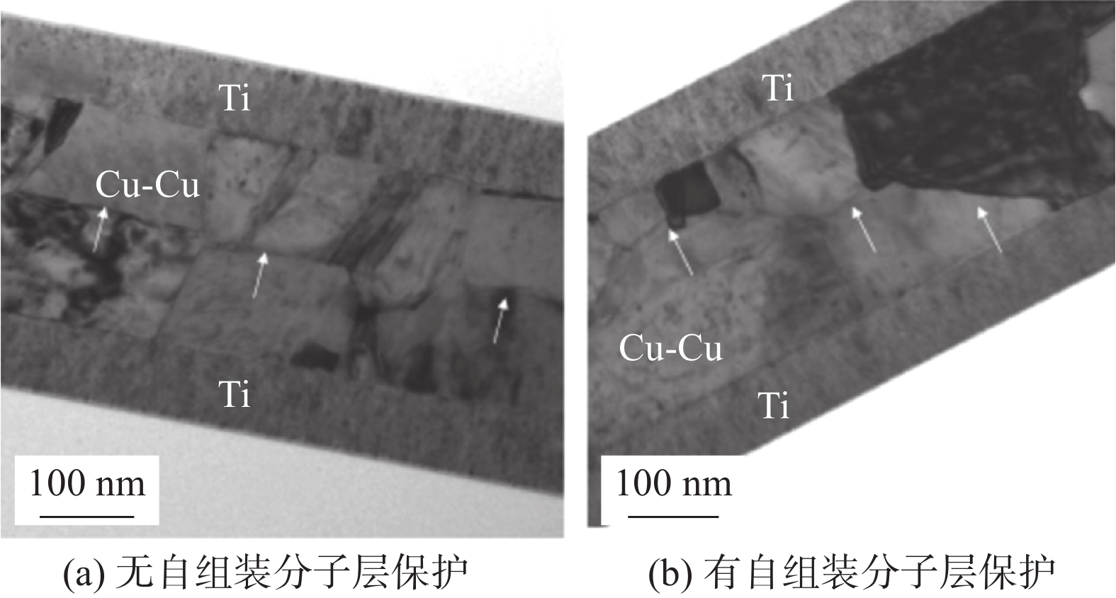
图 10 Cu-Cu键合界面的TEM图像[32]
Figure 10. TEM micrographs of bonded Cu layers. (a) without SAM passivation; (b) with SAM passivation
![]()
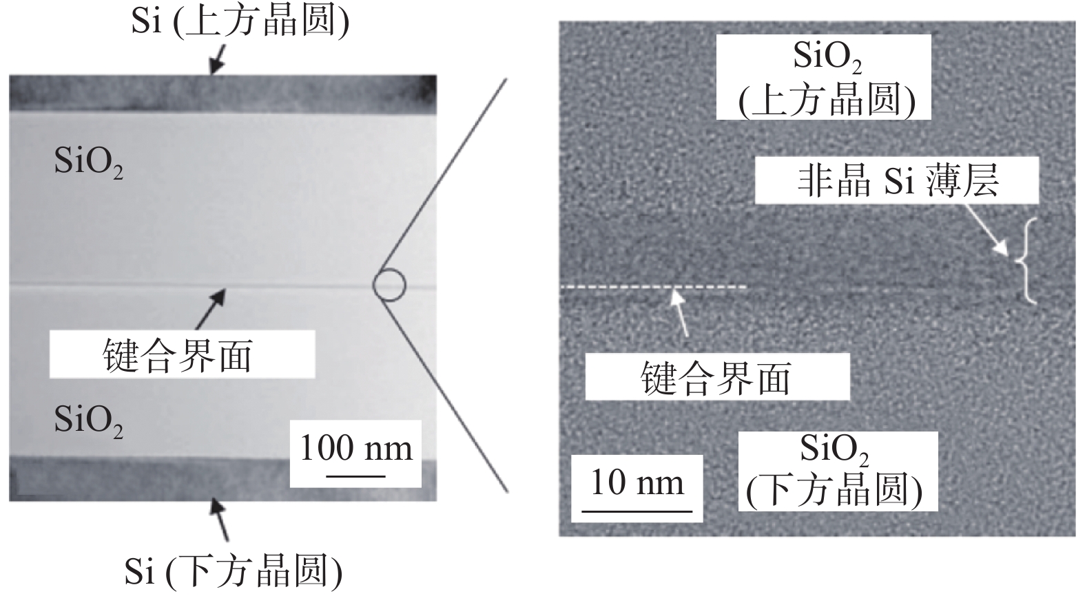
图 14 Si作为SiO2-SiO2室温键合的中间层[44]
Figure 14. Bonding of SiO2 and SiO2 at room temperature using Si ultrathin film
![]()
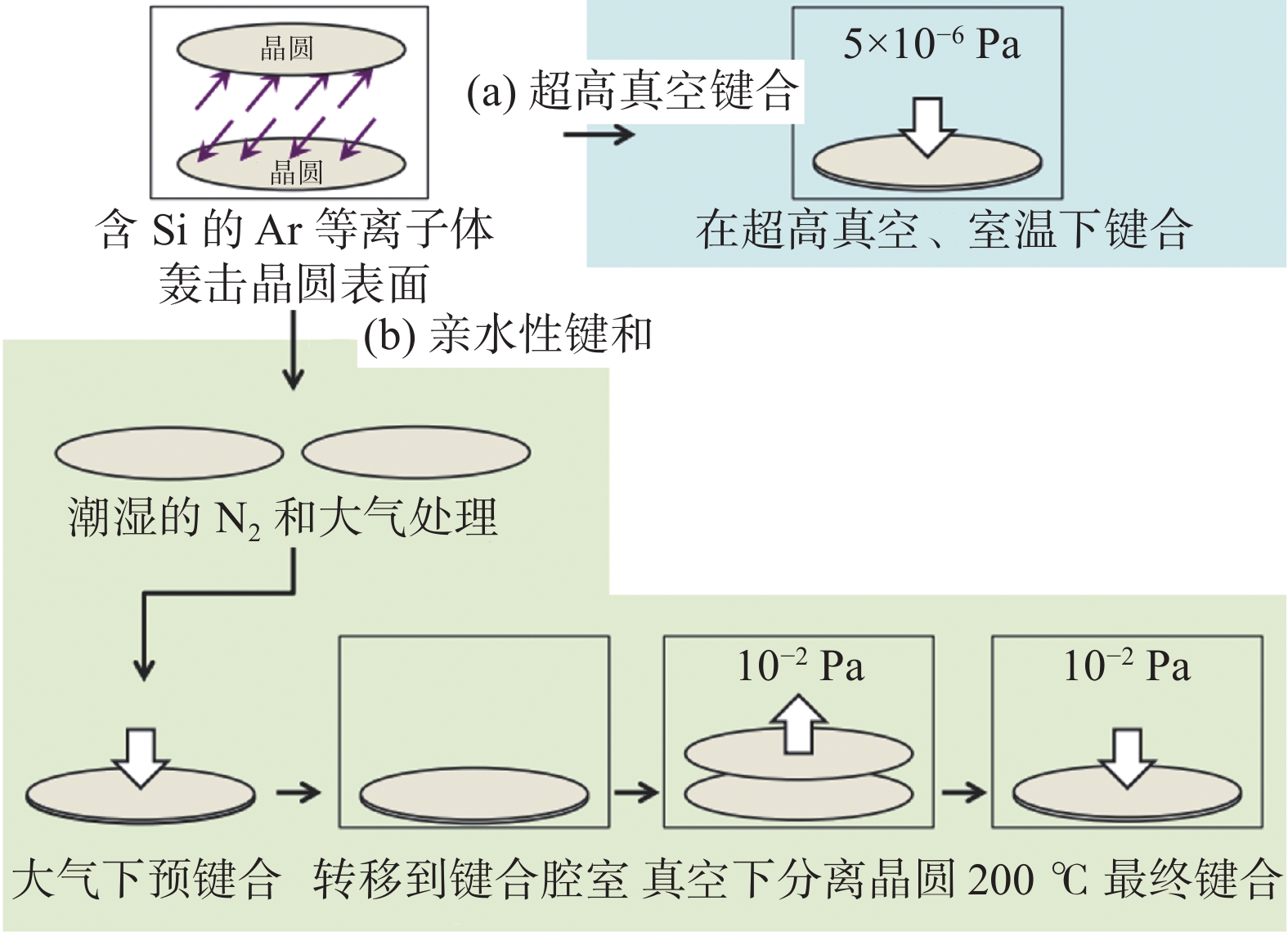
图 15 基于SAB的混合键合流程示意图[46]
Figure 15. Process flow of the combined SAB with (a) UHV bonding and (b) hydrophilic bonding
![]()
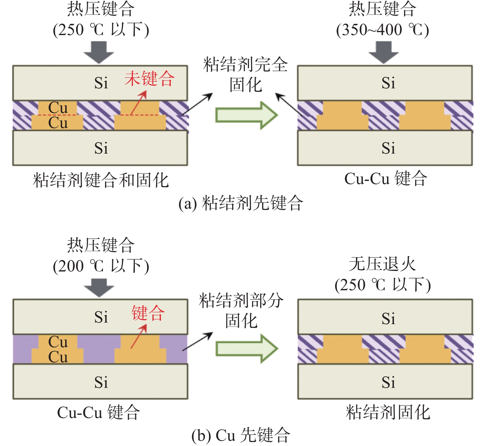
图 17 Cu和粘结剂混合键合方式[50]
Figure 17. Cu/adhesive hybrid bonding. (a) “adhesive-first” hybrid bonding process; (b) “Cu-first” hybrid bonding process
![]()
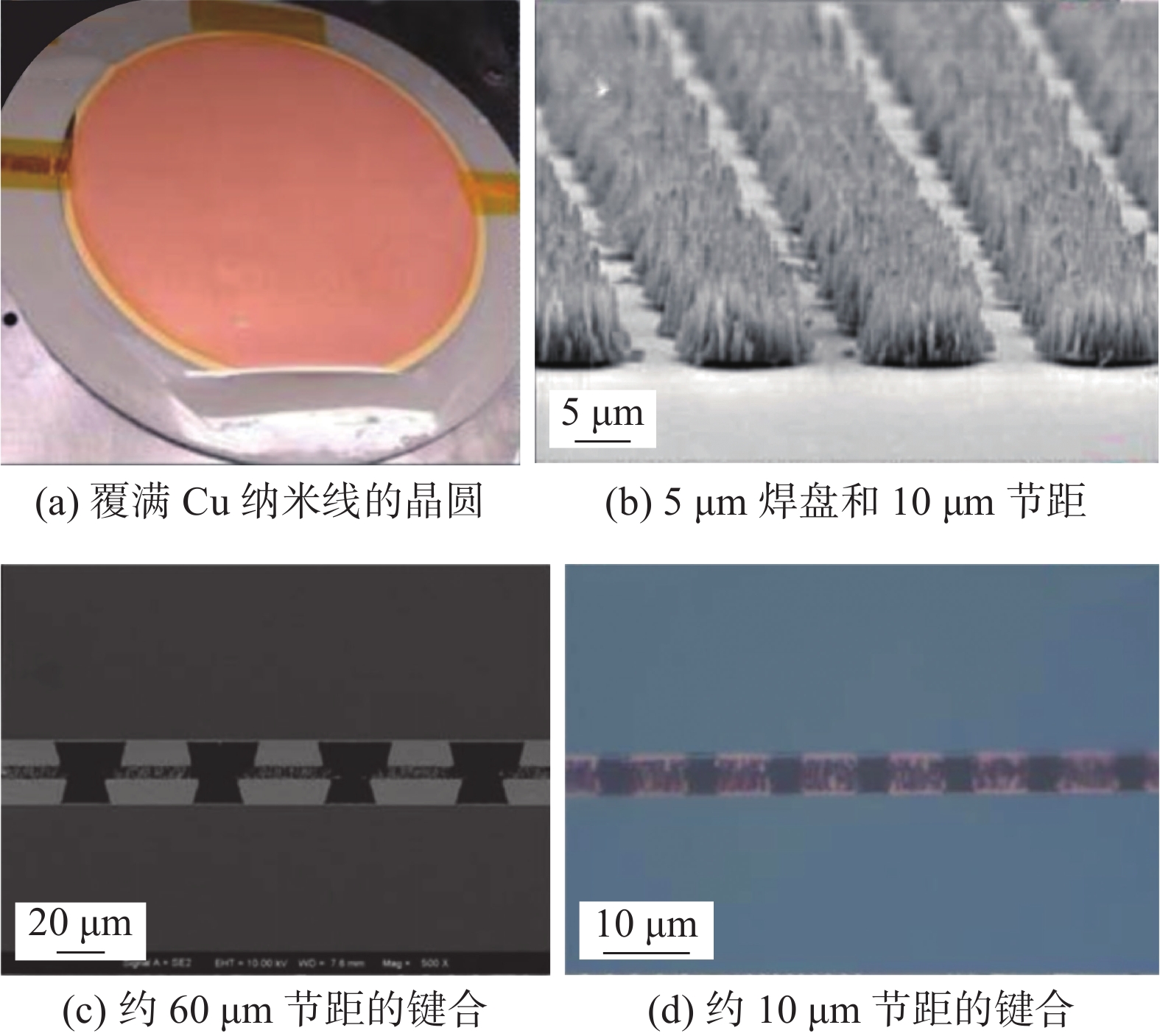
图 19 键合前后的Cu纳米线[56]
Figure 19. Cu nanowires before and after bonding. (a) entire wafer covered with Cu nanowires; (b) 5 μm pads with 10 μm pitch; (c) cross sections of about 60 μm and; (d) 10 μm pitch connected with nanowires
![]()
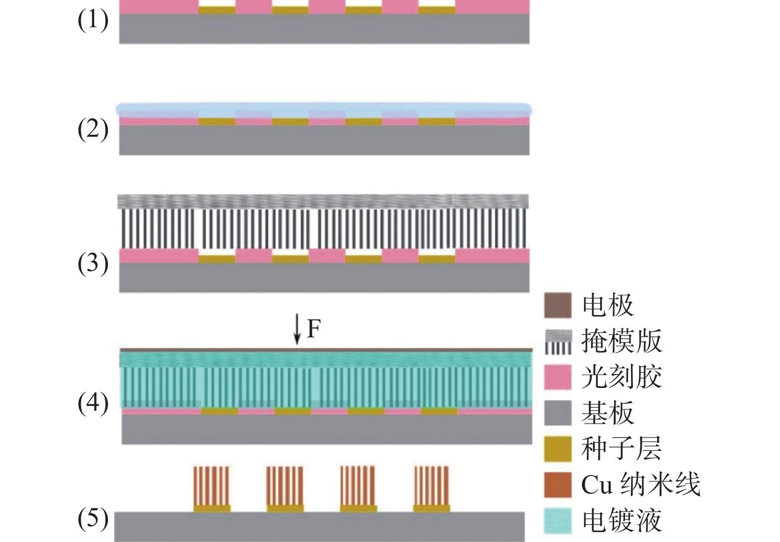
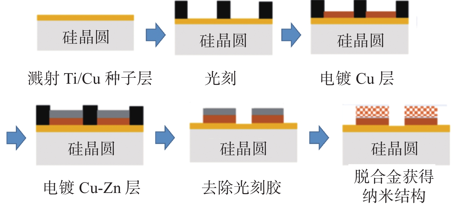
图 20 Cu纳米多孔骨架的图形化路线[62]
Figure 20. Process flow for fabrication of patterned np-Cu foam films
![]()
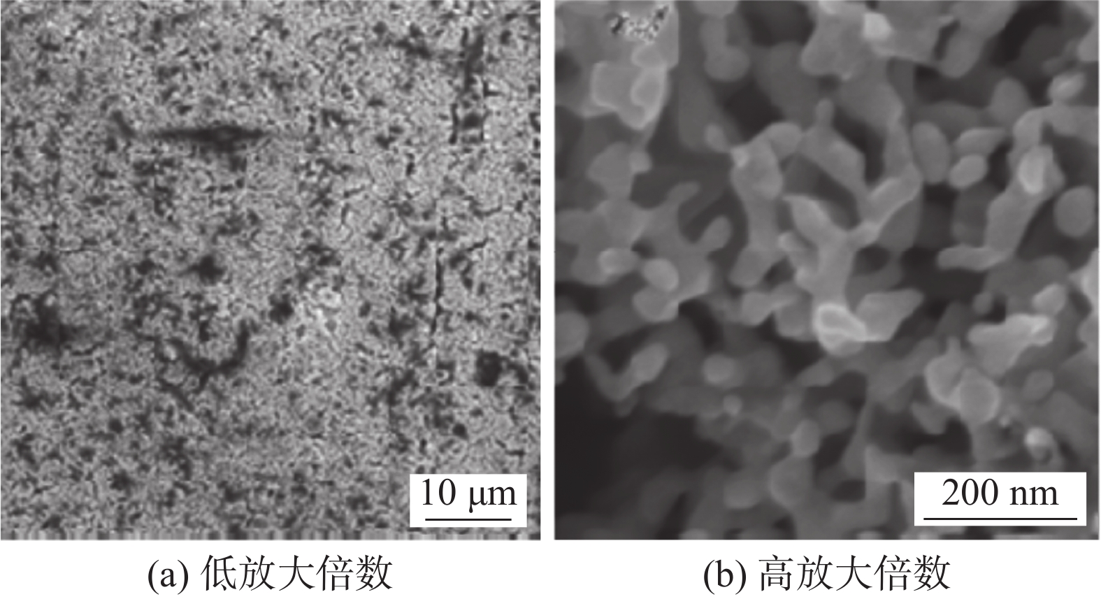
图 21 纳米多孔骨架的组织形态[62]
Figure 21. Morphology of dealloyed np-Cu foam film. (a) low magnification; (b) high magnification
![]()
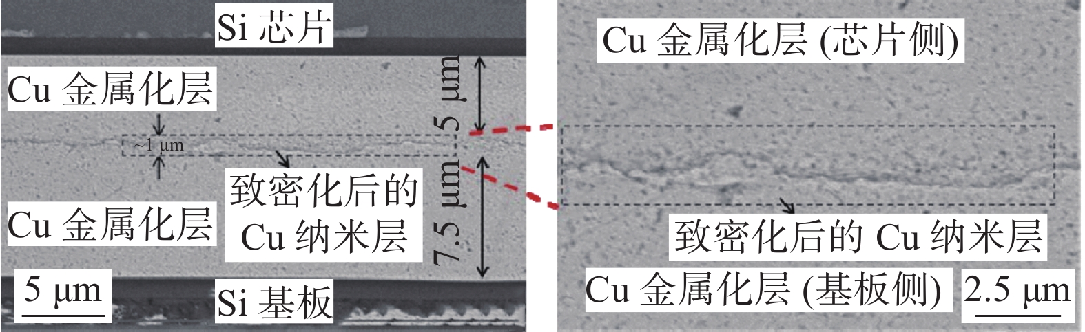
图 22 250 ℃/9 MPa/30 min烧结条件下的键合界面[62]
Figure 22. Cross-sectional images of the sintered joint under the condition of 250 ℃/9 MPa/30 min
![]()
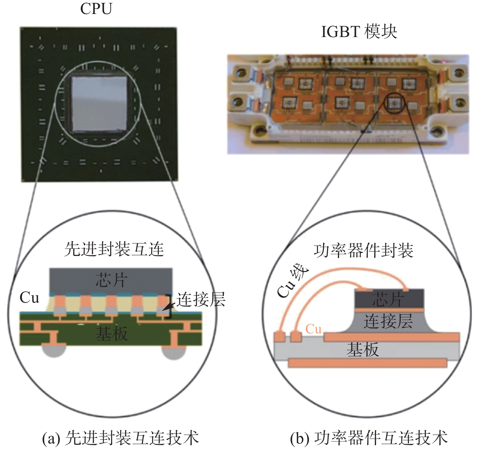
图 23 不同互连技术的示意图[67]
Figure 23. Schematic of different packaging technology. (a) advanced packaging technology; (b) power device packaging technology
![]()
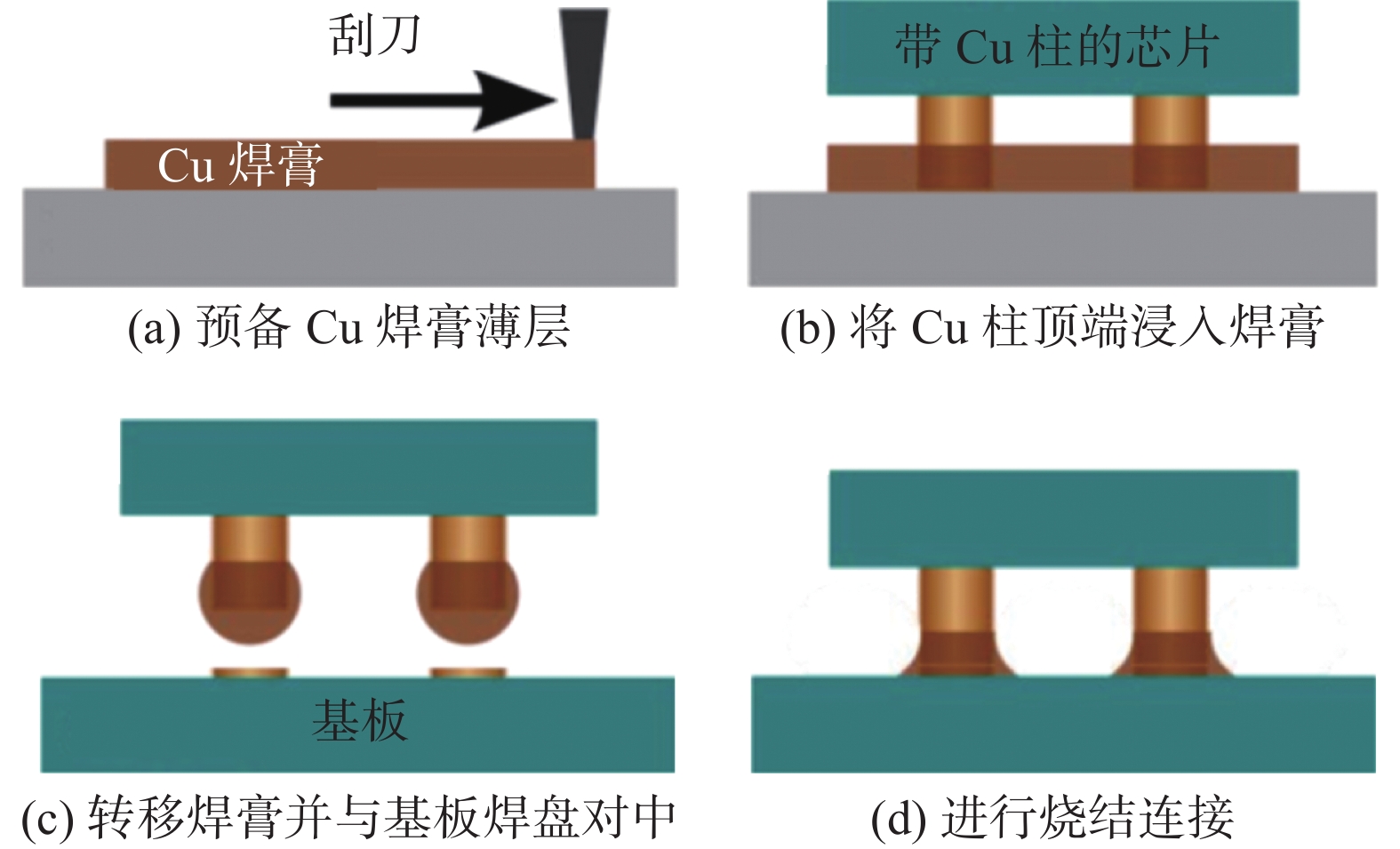
图 24 浸蘸转移法进行焊膏图形化[68]
Figure 24. Process sequence of the dipping method. (a) preparation of a Cu ink film; (b) dip into Cu ink film by Cu pillar chip; (c) ink transfer and alignment to substrate; (d) joint formed by nanoparticle sintering
![]()
图 25 键合压力对接头组织和剪切强度的影响[71]
Figure 25. Effects of bonding pressure on microstructures and interconnect resistance. (a) microstructures; (b) interconnect resistance
-
[1] Moore G E. Cramming more components onto integrated circuits[J]. Proceedings of the IEEE, 1998, 86(1): 82 − 85. doi: 10.1109/JPROC.1998.658762
[2] Waldrop M M. The chips are down for Moore’s law[J]. Nature News, 2016, 530(7589): 144. doi: 10.1038/530144a
[3] Li Y, Goyal D. Introduction to 3D microelectronic packaging[M]. 3D Microelectronic Packaging, Springer, 2021.
[4] Shahane N M. Reliable fine-pitch chip-to-substrate copper interconnections with high-through assembly and high power-handling[D]. Georgia Institute of Technology, 2018.
[5] Miller L F. Controlled collapse reflow chip joining[J]. IBM Journal of Research and Development, 1969, 13(3): 239 − 250. doi: 10.1147/rd.133.0239
[6] Kim J M, Shin Y E, Fujimoto K. Dynamic modeling for resin self-alignment mechanism[J]. Microelectronics Reliability, 2004, 44(6): 983 − 992. doi: 10.1016/j.microrel.2004.01.006
[7] Fang M, Tang C, Chen Y, et al. Thermo-compression bonding process characteristics and shape control of Cu-pillar microbump joints by optimizing of solder melting[J]. Journal of Materials Science: Materials in Electronics, 2022, 33(13): 10471 − 10485. doi: 10.1007/s10854-022-08034-x
[8] Zhang L, Ou S, Huang J, et al. Effect of current crowding on void propagation at the interface between intermetallic compound and solder in flip chip solder joints[J]. Applied Physics Letters, 2006, 88(1): 012106. doi: 10.1063/1.2158702
[9] Wang S, Hsu L, Wang N, et al. EBSD investigation of Cu-Sn IMC microstructural evolution in Cu/Sn-Ag/Cu microbumps during isothermal annealing[J]. Journal of Electronic Materials, 2014, 43(1): 219 − 228. doi: 10.1007/s11664-013-2675-z
[10] Chen K N, Fan A, Tan C, et al. Bonding parameters of blanket copper wafer bonding[J]. Journal of Electronic Materials, 2006, 35(2): 230 − 234. doi: 10.1007/BF02692440
[11] Chen K N, Fan A, Reif R. Microstructure examination of copper wafer bonding[J]. Journal of Electronic Materials, 2001, 30(4): 331 − 335. doi: 10.1007/s11664-001-0039-6
[12] Chen K N, Tan C S, Fan A, et al. Morphology and bond strength of copper wafer bonding[J]. Electrochemical and Solid-State Letters, 2004, 7(1): G14. doi: 10.1149/1.1626994
[13] Grayson A C R, Cima M J, Langer R. Size and temperature effects on poly (lactic-co-glycolic acid) degradation and microreservoir device performance[J]. Biomaterials, 2005, 26(14): 2137 − 2145. doi: 10.1016/j.biomaterials.2004.06.033
[14] Juang J Y, Lu C L, Chen K J, et al. Copper-to-copper direct bonding on highly (111)-oriented nanotwinned copper in no-vacuum ambient[J]. Scientific Reports, 2018, 8(1): 13910. doi: 10.1038/s41598-018-32280-x
[15] Juang J Y, Lu C L, Li Y J, et al. A solid state process to obtain high mechanical strength in Cu-to-Cu joints by surface creep on (111)-oriented nanotwins Cu[J]. Journal of Materials Research and Technology, 2021, 14: 719 − 730. doi: 10.1016/j.jmrt.2021.06.099
[16] Shie K C, Juang J Y, Chen C. Instant Cu-to-Cu direct bonding enabled by (111)-oriented nanotwinned Cu bumps[J]. Japanese Journal of Applied Physics, 2020, 59(SB): SBBA03. doi: 10.7567/1347-4065/ab5697
[17] Ong J J, Shie K C, Tu K N, et al. Two-step fabrication process for die-to-die and die-to-wafer Cu-Cu bonds[C]//2021 IEEE 71th Electronic Components and Technology Conference (ECTC), 2021: 203 − 210.
[18] Liu C M, Lin H W, Huang Y S, et al. Low-temperature direct copper-to-copper bonding enabled by creep on (111) surfaces of nanotwinned Cu[J]. Scientific Reports, 2015, 5(1): 1 − 11. doi: 10.9734/JSRR/2015/14076
[19] Sakai T, Imaizumi N, Miyajima T. Low temperature Cu-Cu direct bonding for 3D-IC by using fine crystal layer[C]//2012 2nd IEEE Transactions on Components, Packaging and Manufacturing Technology Symposium Japan, 2012: 1 − 4.
[20] Al Farisi M S, Hirano H, Tanaka S. Low-temperature hermetic thermo-compression bonding using electroplated copper sealing frame planarized by fly-cutting for wafer-level MEMS packaging[J]. Sensors and Actuators A: Physical, 2018, 279: 671 − 679. doi: 10.1016/j.sna.2018.06.021
[21] Yang Y T, Chou T C, Yu T Y, et al. Low-temperature Cu-Cu direct bonding using pillar–concave structure in advanced 3-D heterogeneous integration[J]. IEEE Transactions on Components, Packaging and Manufacturing Technology, 2017, 7(9): 1560 − 1566. doi: 10.1109/TCPMT.2017.2720468
[22] Chou T C, Yang K M, Li J C, et al. Investigation of pillar–concave structure for low-temperature Cu–Cu direct bonding in 3D/2.5D heterogeneous integration[J]. IEEE Transactions on Components, Packaging and Manufacturing Technology, 2020, 10(8): 1296 − 1303. doi: 10.1109/TCPMT.2020.3004969
[23] Takagi H, Kikuchi K, Maeda R, et al. Surface activated bonding of silicon wafers at room temperature[J]. Applied Physics Letters, 1996, 68(16): 2222 − 2224. doi: 10.1063/1.115865
[24] Suga T, Mu F. Surface activated bonding method for low temperature bonding[C]// 2018 7th Electronic System-Integration Technology Conference (ESTC), 2018: 1 − 4.
[25] Shigetou A, Itoh T, Sawada K, et al. Bumpless interconnect of 6-μm-pitch Cu electrodes at room temperature[J]. IEEE Transactions on Advanced Packaging, 2008, 31(3): 473 − 478. doi: 10.1109/TADVP.2008.920644
[26] Huang Y P, Chien Y S, Tzeng R N, et al. Novel Cu-to-Cu bonding with Ti passivation at 180 ℃ in 3D integration[J]. IEEE Electron Device Letters, 2013, 34(12): 1551 − 1553. doi: 10.1109/LED.2013.2285702
[27] Panigrahi A K, Bonam S, Ghosh T, et al. Ultra-thin Ti passivation mediated breakthrough in high quality Cu-Cu bonding at low temperature and pressure[J]. Materials Letters, 2016, 169: 269 − 272. doi: 10.1016/j.matlet.2016.01.126
[28] Liu D, Chen P C, Chou T C, et al. Demonstration of low-temperature fine-pitch Cu/SiO hybrid bonding by Au passivation[J]. IEEE Journal of the Electron Devices Society, 2021, 9: 868 − 875. doi: 10.1109/JEDS.2021.3114648
[29] Chou T C, Huang S Y, Chen P J, et al. Electrical and reliability investigation of Cu-to-Cu bonding with silver passivation layer in 3D integration[J]. IEEE Transactions on Components, Packaging and Manufacturing Technology, 2020, 11(1): 36 − 42.
[30] Hong Z J, Liu D, Hu H W, et al. Ultra-High strength Cu-Cu bonding under low thermal budget for chiplet heterogeneous applications[C]// 2021 IEEE 71st Electronic Components and Technology Conference (ECTC), 2021: 347 − 352.
[31] Peng L, Zhang L, Fan J, et al. Ultrafine pitch (6 μm) of recessed and bonded Cu–Cu interconnects by three-dimensional wafer stacking[J]. IEEE Electron Device Letters, 2012, 33(12): 1747 − 1749. doi: 10.1109/LED.2012.2218273
[32] Tan C S, Lim D F, Singh S G, et al. Cu–Cu diffusion bonding enhancement at low temperature by surface passivation using self-assembled monolayer of alkane-thiol[J]. Applied Physics Letters, 2009, 95(19): 192108. doi: 10.1063/1.3263154
[33] Di Cioccio L, Gueguen P, Taibi R, et al. An overview of patterned metal/dielectric surface bonding: mechanism, alignment and characterization[J]. Journal of the Electrochemical Society, 2011, 158(6): 81. doi: 10.1149/1.3577596
[34] Moriceau H, Rieutord F, Fournel F, et al. Low temperature direct bonding: An attractive technique for heterostructures build-up[J]. Microelectronics Reliability, 2012, 52(2): 331 − 41. doi: 10.1016/j.microrel.2011.08.004
[35] Liang D, Fang A W, Park H, et al. Low-temperature, strong SiO2-SiO2 covalent wafer bonding for III–V compound semiconductors-to-silicon photonic integrated circuits[J]. Journal of Electronic Materials, 2008, 37(10): 1552 − 1559. doi: 10.1007/s11664-008-0489-1
[36] Baklanov M, Shamiryan D, Tökei Z, et al. Characterization of Cu surface cleaning by hydrogen plasma[J]. Journal of Vacuum Science & Technology B: Microelectronics and Nanometer Structures Processing, Measurement, and Phenomena, 2001, 19(4): 1201 − 1211.
[37] Écija D, Gallego J M, Miranda R. The adsorption of atomic N and the growth of copper nitrides on Cu (1 0 0)[J]. Surface Science, 2009, 603(15): 2283 − 2289. doi: 10.1016/j.susc.2009.04.039
[38] Ito F, Shobha H, Tagami M, et al. Effective Cu surface pre-treatment for high-reliable 22 nm-node Cu dual damascene interconnects with high plasma resistant ultra low-k dielectric (k= 2.2)[J]. Microelectronic Engineering, 2012, 92: 62 − 66. doi: 10.1016/j.mee.2011.01.077
[39] Park M, Baek S, Kim S, et al. Argon plasma treatment on Cu surface for Cu bonding in 3D integration and their characteristics[J]. Applied Surface Science, 2015, 324: 168 − 173. doi: 10.1016/j.apsusc.2014.10.098
[40] 王晨曦, 王特, 许继开, 等. 晶圆直接键合及室温键合技术研究进展[J]. 精密成形工程, 2018, 10(1): 67 − 73. doi: 10.3969/j.issn.1674-6457.2018.01.008 Wang Chenxi, Wang Te, Xu Jikai, et al. Research progress of wafer direct bonding and room-temperature bonding technology[J]. Journal of Netshape Forming Engineering, 2018, 10(1): 67 − 73. doi: 10.3969/j.issn.1674-6457.2018.01.008
[41] Ko C T, Chen K N. Low temperature bonding technology for 3D integration[J]. Microelectronics Reliability, 2012, 52(2): 302 − 311. doi: 10.1016/j.microrel.2011.03.038
[42] Enquist P, Fountain G, Petteway C, et al. Low cost of ownership scalable copper direct bond interconnect 3D IC technology for three dimensional integrated circuit applications[C]//2009 IEEE International Conference on 3D System Integration, 2009: 1 − 6.
[43] Gao G, Mirkarimi L, Workman T, et al. Development of low temperature direct bond interconnect technology for die-to-wafer and die-to-die applications-stacking, yield improvement, reliability assessment[C]//2018 IEEE International Wafer Level Packaging Conference (IWLPC), 2018: 1 − 7.
[44] Utsumi J, Ide K, Ichiyanagi Y. Bonding of SiO2 and SiO2 at room temperature using Si ultrathin film[J]. ECS Transactions, 2016, 75(9): 355 − 361. doi: 10.1149/07509.0355ecst
[45] Utsumi J, Ide K, Ichiyanagi Y. Cu/SiO2 hybrid bonding obtained by surface-activated bonding method at room temperature using Si ultrathin films[J]. Micro and Nano Engineering, 2019, 2: 1 − 6. doi: 10.1016/j.mne.2018.11.004
[46] He R, Fujino M, Yamauchi A, et al. Combined surface activated bonding technique for low-temperature Cu/dielectric hybrid bonding[J]. Journal of Solid State Science and Technology, 2016, 5(7): 419. doi: 10.1149/2.0201607jss
[47] Hsiao Z C, Ko C T, Chang H H, et al. Cu/BCB hybrid bonding with TSV for 3D integration by using fly cutting technology[C]// 2015 International Conference on Electronics Packaging and iMAPS All Asia Conference (ICEP-IAAC), 2015: 834 − 837.
[48] Takeda K, Aoki M. 3D integration technology using hybrid wafer bonding and via-last TSV process[C]// 2014 IEEE International Interconnect Technology Conference, 2014: 211 − 214.
[49] Yu R, Liu F, Polastre R, et al. Reliability of a 300-mm-compatible 3DI technology based on hybrid Cu-adhesive wafer bonding[C]//2009 Symposium on VLSI Technology, 2009: 170 − 171.
[50] He R, Fujino M, Akaike M, et al. Combined surface activated bonding using H-containing HCOOH vapor treatment for Cu/Adhesive hybrid bonding at below 200 °C[J]. Applied Surface Science, 2017, 414: 163 − 170. doi: 10.1016/j.apsusc.2017.03.168
[51] He R, Suga T. Effects of Ar plasma and Ar fast atom bombardment (FAB) treatments on Cu/polymer hybrid surface for wafer bonding[C]//2014 International Conference on Electronics Packaging (ICEP), 2014: 78 − 81.
[52] Kagawa Y, Fujii N, Aoyagi K, et al. Novel stacked CMOS image sensor with advanced Cu2Cu hybrid bonding[C]//2016 IEEE International Electron Devices Meeting (IEDM), 2016: 8.4.1 − 8.4.4.
[53] Buffat P, Borel J P. Size effect on the melting temperature of gold particles[J]. Physical Review A, 1976, 13(6): 2287 − 2298. doi: 10.1103/PhysRevA.13.2287
[54] Feng B, Shen D, Wang W, et al. Cooperative bilayer of lattice-disordered nanoparticles as room-temperature sinterable nanoarchitecture for device integrations[J]. ACS Applied Materials & Interfaces, 2019, 11(18): 16972 − 16980.
[55] Roustaie F, Quednau S, Dassinger F, et al. Room temperature interconnection technology for bonding fine pitch bumps using NanoWiring, KlettWelding, KlettSintering and KlettGlueing[C]//2020 15th International Microsystems, Packaging, Assembly and Circuits Technology Conference (IMPACT), 2020: 168 − 171.
[56] Roustaie F, Quednau S, Weissenborn F, et al. Room temperature KlettWelding interconnect technology for high performance CMOS logic[C]//2021 IEEE 71st Electronic Components and Technology Conference (ECTC), 2021: 371 − 376.
[57] Strahringer D, Roustaie F, Weissenborn F, et al. Optimizing the Nano Wiring and KlettSintering parameters for low-temperature die to DCB attach of power electronic chips[C]//2021 16th International Microsystems, Packaging, Assembly and Circuits Technology Conference (IMPACT), 2021: 31 − 34.
[58] Yu Z, Tan Y Z, Bayer C F, et al. Cu-Cu Thermocompression bonding with Cu-nanowire films for power semiconductor die-attach on DBC substrates[C]//2021 IEEE 23rd Electronics Packaging Technology Conference (EPTC), 2021: 1 − 7.
[59] Shahane N, Mohan K, Behera R, et al. Novel high-temperature, high-power handling all-Cu interconnections through low-temperature sintering of nanocopper foams[C]//2016 IEEE 66th Electronic Components and Technology Conference (ECTC), 2016: 829 − 836.
[60] Sosa R A, Mohan K, Antoniou A, et al. Low-temperature all-Cu interconnections formed by pressure-less sintering of Cu-pillars with nanoporous-Cu caps[C]//2021 IEEE 71st Electronic Components and Technology Conference (ECTC), 2021: 390 − 394.
[61] Shahane N, Mohan K, Ramos G, et al. Enabling chip-to-substrate all-Cu interconnections: design of engineered bonding interfaces for improved manufacturability and low-temperature bonding[C]//2017 IEEE 67th Electronic Components and Technology Conference (ECTC), 2017: 968 − 975.
[62] Mohan K, Shahane N, Sosa R A, et al. Demonstration of patternable all-Cu compliant interconnections with enhanced manufacturability in chip-to-substrate applications[C]//2018 IEEE 68th Electronic Components and Technology Conference (ECTC), 2018: 301 − 307.
[63] Sosa R A, Mohan K, Nguyen L, et al. Cu pillar with nanocopper caps: the next interconnection node beyond traditional Cu pillar[C]//2019 IEEE 69th Electronic Components and Technology Conference (ECTC), 2019: 655 − 660.
[64] Zhang B, Damian A, Zijl J, et al. In-air sintering of copper nanoparticle paste with pressure-assistance for die attachment in high power electronics[J]. Journal of Materials Science: Materials in Electronics, 2021, 32(4): 4544 − 4555. doi: 10.1007/s10854-020-05196-4
[65] 李俊龙, 徐杨, 赵雪龙, 等. 铜颗粒低温烧结技术的研究进展[J]. 焊接学报, 2022, 43(3): 13 − 24. Li Junlong, Xuyang, Zhao Xuelong, et al. Research progress of low temperature sintering technology for Cu particles[J]. Transactions of the China Welding Institution, 2022, 43(3): 13 − 24.
[66] Guo R, Xiao Y, Gao Y, et al. Interfacial enhancement of Ag and Cu particles sintering using (111)-oriented nanotwinned Cu as substrate for die-attachment[J]. China Welding, 2022, 31(1): 22 − 28.
[67] Del Carro L. Sintering of copper nanoparticle pastes for microelectronic packaging[D]. Swiss Federal Institute of Technology in Zurich, 2018.
[68] Del Carro L, Kossatz M, Schnackenberg L, et al. Laser sintering of dip-based all-copper interconnects[C]//2018 IEEE 68th Electronic Components and Technology Conference (ECTC), 2018: 279 − 286.
[69] Del Carro L, Zürcher J, Drechsler U, et al. Low-temperature dip-based all-copper interconnects formed by pressure-assisted sintering of copper nanoparticles[J]. IEEE Transactions on Components, Packaging and Manufacturing Technology, 2019, 9(8): 1613 − 1622. doi: 10.1109/TCPMT.2019.2891111
[70] Zürcher J, Yu K, Schlottig G, et al. Nanoparticle assembly and sintering towards all-copper flip chip interconnects[C]//2015 IEEE 65th Electronic Components and Technology Conference (ECTC), 2015: 1115 − 1121.
[71] Zürcher J, Del Carro L, Schlottig G, et al. All-copper flip chip interconnects by pressureless and low temperature nanoparticle sintering[C]//2016 IEEE 66th Electronic Components and Technology Conference (ECTC), 2016: 343 − 349.
[72] Mimatsu H, Mizuno J, Kasahara T, et al. Low-temperature gold-gold bonding using selective formation of nanoporous powders for bump interconnects[C]//2014 IEEE 27th International Conference on Micro Electro Mechanical Systems (MEMS), 2014: 1131 − 1134.
-
期刊类型引用(1)
1. 王晨,雷正龙,宋文清,杨烁,李旭东. CoCrW与T800焊丝对DZ125高温合金表面激光熔覆耐磨层组织及性能的影响. 中国激光. 2025(04): 101-109 .  百度学术
百度学术
其他类型引用(3)

 下载:
下载:


计量
- 文章访问数: 1421
- HTML全文浏览量: 332
- PDF下载量: 329
- 被引次数: 4
