
-
摘要: 纳米铜基导电薄膜具有高导电、高性价比且易与柔性基材结合等优点,在下一代柔性电子产品领域具有广泛的应用前景. 然而,纳米铜基导电薄膜在制备的过程中易被氧化,成为制备高导电纳米铜基导电薄膜的难题. 文中从油墨配方、印刷方法、烧结方法等方面系统的介绍了纳米铜基柔性导电薄膜的制造方法,着重介绍了目前抗氧化油墨的设计思路,阐明了目前柔性电子先进微纳连接技术的工艺流程,对比了其优缺点及适用范围,并列举了纳米铜基导电薄膜在下一代柔性电子产品领域的典型应用. 在此基础上,对纳米铜柔性导电薄膜制造尚存的主要问题进行了总结,并对其未来发展趋势进行了展望.
-
0. 序言
激光焊接的薄板十字结构由于其工艺性易出现未熔合、未焊透等缺陷,严重影响构件的使用性能,因此有效识别十字焊接接头的内部缺陷十分必要. 由于检测盲区的存在,常规超声检测无法实现对薄板的检测,Lamb波因其传播速度快、距离长、成本低,已广泛地用于板状结构、大型管道等的无损检测和评价中[1-2]. 然而Lamb波因存在多模态、频散特性,以及检测机理的复杂性,Lamb波检测技术仍存在很多不一致的观点,如Lamb波与不同缺陷、不同结构的作用机理对缺陷的表征等.
目前针对薄板Lamb检测国内外已经有大量研究. 英国谢菲尔德大学Lee等人[3]模拟了A0和S0模态Lamb波在铝板中的传播和与槽类缺陷的相互作用,土耳其马尔马拉大学Senyurek等人[4]采用Lamb波有效检测出飞机机翼板的切口损伤及冲击损伤. 哈尔滨工业大学的刚铁等人[5]采用有限元方法模拟并验证了A0波、S0波识别薄板槽类缺陷的可行性. 对于焊接结构缺陷的Lamb波检测国内外研究并不多. 贝鲁特美国大学Hamade等人[6]、Fakih等人[7]研究了Lamb波用于搅拌摩擦焊对接接头焊缝内部缺陷的检测与评估,建立了基于回波信号幅值的损伤指数. 国内对焊接结构中的缺陷识别及表征方面研究较多[8-10],采用Lamb波方法识别焊接结构缺陷的研究较少,哈尔滨工业大学的刘磊等人[11]实现了对复杂薄壁结构钎焊接头的检测.
文中首先采用有限元分析方法仿真了A0和S0模态Lamb波与缺陷的作用结果,并在此基础上,通过试验方法找到不同模态Lamb波的最佳入射点和激励角度,最后探讨了A0和S0模态Lamb波用于识别薄板十字焊接结构未焊透缺陷及缺陷尺寸表征的可行性.
1. 试件制备
实际焊接试件是由两块薄板侧面开槽后相互交叉焊接而成,一般有两道焊缝,均为十字接头角焊缝. 其焊接缺陷主要为未焊透. 焊件如图1所示. 对于无缺陷焊件则采取四束激光分别从两侧上下倾斜45°进行焊接,以保证全焊透. 该焊件材料为1Cr18Ni9Ti不锈钢,焊件总长度为240 mm,十字焊接接头至板端距离为50 mm,板厚为1.9 mm.
![]() 图 1 焊接试件的制备Figure 1. Preparation for welding specimen. (a) schematic diagram of sample geometry and defects ; (b) welding specimen
图 1 焊接试件的制备Figure 1. Preparation for welding specimen. (a) schematic diagram of sample geometry and defects ; (b) welding specimen2. 数值仿真分析
采用有限元分析方法构建数值仿真模型,其几何模型尺寸及结构与实际焊接试件一致,模型中的缺陷长度分别为0.4,0.8,1.2 mm,缺陷宽度均为0.01 mm,有限元材料各向同性,材料属性中的密度、弹性模量、泊松比参数依次为7 850 kg/m3,210 GPa,0.3.
通过波结构分析可知,A0和S0模态波在板的上下表面处的面内位移即切向位移为零,离面位移即法向位移达到最大值[12],因此模拟计算采用不同离面位移方式进行加载,且模型边界设为自由边界. 仿真激励信号采用经汉宁窗函数调制的单频5个周期叠加信号,与试验所用的正弦电压信号相同,且时频特征一致.
考虑到试验时采用单探头自发自收脉冲回波法,有限元分析取距板左端90 mm,即距缺陷处40 mm位置作为入射点,信号接收点为距入射点沿着声波传播方向的5 mm位置处,以避免由于激励信号具有一定时间宽度而造成信号干扰.
与实际焊接试样检测一样,通过有限元方法在相同入射点处分别激励出单一模态的A0和S0波,并模拟了不同波形在无缺陷模型和不同缺陷长度模型中的传播过程,得到了缺陷尺寸与回波反射系数的关系,如图2所示. 由该图可知,A0与未焊透缺陷尺寸呈良好线性关系,能够对缺陷长度0.4 mm以上的未焊透缺陷进行尺寸表征,而S0波回波幅值变化不大,难以检测十字结构中的未焊透缺陷.
![]() 图 2 缺陷尺寸与回波反射系数的关系(A0/S0)Figure 2. Relationship between defect size and reflection coefficient(A0/S0)
图 2 缺陷尺寸与回波反射系数的关系(A0/S0)Figure 2. Relationship between defect size and reflection coefficient(A0/S0)3. 试验方法
3.1 A0和S0波的激励
试验采用PAC自动超声扫描成像检测系统进行,采用中心频率为2.5 MHz在0° ~ 80°间变化的可变角探头,其晶片材料为钛酸铅、尺寸为10 mm × 10 mm,压电应变常数为125 ~ 190/(10−12 m/V),采样频率100 MHz,延迟2 μs,固定增益35 dB,耦合方式为机油. 采用单探头自发自收脉冲回波法.
3.1.1 入射点的确定
在理想状态下,声束沿着矩形晶片中心轴线向前传播,在近场区声束呈四棱锥形,在远场区声束发生一定范围的扩散.
将声束中心轴线入射到待检试件的相交点,称为几何入射点,即理论入射点. 随着入射角度的增大,仅有部分声束能进入试件,此时将声束通过探头底面的中点作为几何入射点. 探头入射点位置的准确性影响缺陷的定性、定位,采用入射点至探头前边缘的距离进行描述. 探头所接收到的信号反映是所有回到晶片声线的整体效应,这就有必要引入实测入射点的概念,其测量一般借助标准CSK-IA试块,即使得声束在100 mm半径的圆弧面产生反射,当探头接收到的回波达到最高时,认为探头底面上与圆弧圆心重合点即为实际入射点.
由于可变角度探头的入射点与入射角度密切相关,因此确定不同模态板波的理论入射点和实测入射点更加必要. 图3给出了探头理论入射点、实测入射点与入射角度的关系,实测入射点整体上比几何入射点约大5 mm. 当入射角度大于第二临界角时,标准试块内声波主要为表面波,此时难以确定实测入射点,可根据图3实测入射点与理论入射点的关系进行几何外推.
3.1.2 入射角度的确定
Lamb波一般采用纵波透过有机玻璃斜入射方式进行激励,入射角α为
$$ \sin \alpha {\text{ = }}C_{\rm{l}}/C_{\rm{p}} $$ 式中:Cl为有机玻璃中的纵波声速(一般取2 730 m/s);Cp为Lamb波的相速度.
由Lamb相速度、频速度频散曲线可进一步求出,频厚积为4.75 MHz·mm(即频率与板厚的乘积)时,不同模态波形的相应相速度、群速度以及理论入射角. 将探头分别置于其入射点至板边缘40,80 mm处的无缺陷不锈钢钢板上,将入射角度从0°开始每间隔5°逐渐增大至80°,以板端回波信号的幅度为参考,可获得不同模态回波的幅度与入射角关系,如图4所示. 由该图可知,A0和S0模态波幅值最高,模态相对单一,结合频散曲线可知S2,S1和A1模态波群速度在频带宽度0.5 MHz即频厚积为0.95 MHz·mm范围内波动相对A0和S0模态波波动较大,随着波形的传播波形更宽幅值更低,且S1模态波单一性最差.
![]() 图 4 不同模态回波幅度与入射角的关系Figure 4. Relationship between signal amplitude of different modal Lamb waves and incident angles
图 4 不同模态回波幅度与入射角的关系Figure 4. Relationship between signal amplitude of different modal Lamb waves and incident angles3.2 A0和S0波的检测
用激励出的A0和S0模态板波,检测无缺陷试件(0号)及不同长度未焊透缺陷的焊接试件(1号、2号、3号),其中A0波检测3号焊件的缺陷回波信号如图5a所示. 对40 ~ 60 μs时域范围内缺陷回波信号进行小波变换获得相应时频图谱,如图5b所示. 该缺陷信号主要时域范围为44 ~ 49 μs,频率主要集中在2.0 ~ 3.0 MHz区间,由群速度频散曲线可初步判断该信号主要为A0波. 对试验中4个焊件的十字焊接结构剖面进行金相观察,其中3号焊件缺陷处金相如图5c所示,其未焊透长度约为1.6 mm.0号试件未观察到未焊透缺陷,1号试件有未焊透缺陷,其长度约为1.4 mm,2号试件有两处未焊透缺陷,其长度均约为0.8 mm.
![]() 图 5 A0波检测实际焊件Figure 5. A0 mode Lamb wave detecting welded samples defect. (a) defect echo sigmal; (b) the time frequency graph of WT; (c) metallographic diagram of welded sample
图 5 A0波检测实际焊件Figure 5. A0 mode Lamb wave detecting welded samples defect. (a) defect echo sigmal; (b) the time frequency graph of WT; (c) metallographic diagram of welded sample将A0和S0模态波检测不同焊件的实测回波峰值转化为反射系数,可得到缺陷回波反射系数与缺陷尺寸关系,如图6所示. 由该图可知,A0波检测的缺陷回波系数与未焊透长度呈良好正向线性关系,而S0波无此规律. 因此,采用2.5 MHz的A0波识别十字焊接结构未焊透尺寸具有良好可行性.
![]() 图 6 缺陷尺寸与回波反射系数关系Figure 6. Relationship between defect size and reflection coefficient
图 6 缺陷尺寸与回波反射系数关系Figure 6. Relationship between defect size and reflection coefficient4. 结论
(1) 仿真结合试验,确定了不同模态Lamb波的入射点、激励角度,探讨了A0和S0模态Lamb波用于识别1.9 mm厚薄板十字交叉激光焊接结构未焊透缺陷的可行性,并获得了超声Lamb波反射系数与缺陷尺寸的关系,仿真结果和试验实测结果的趋势具有较好的一致性.
(2) 采用2.5 MHz的A0模态波能够有效检测十字焊接结构中的未焊透缺陷,且可一定程度上表征缺陷的尺寸.
(3) 采用2.5 MHz的S0模态波检测十字焊接结构,其反射系数与缺陷尺寸相关性较差,不易于识别结构中未焊透缺陷.
-
![]()
![]()
![]()
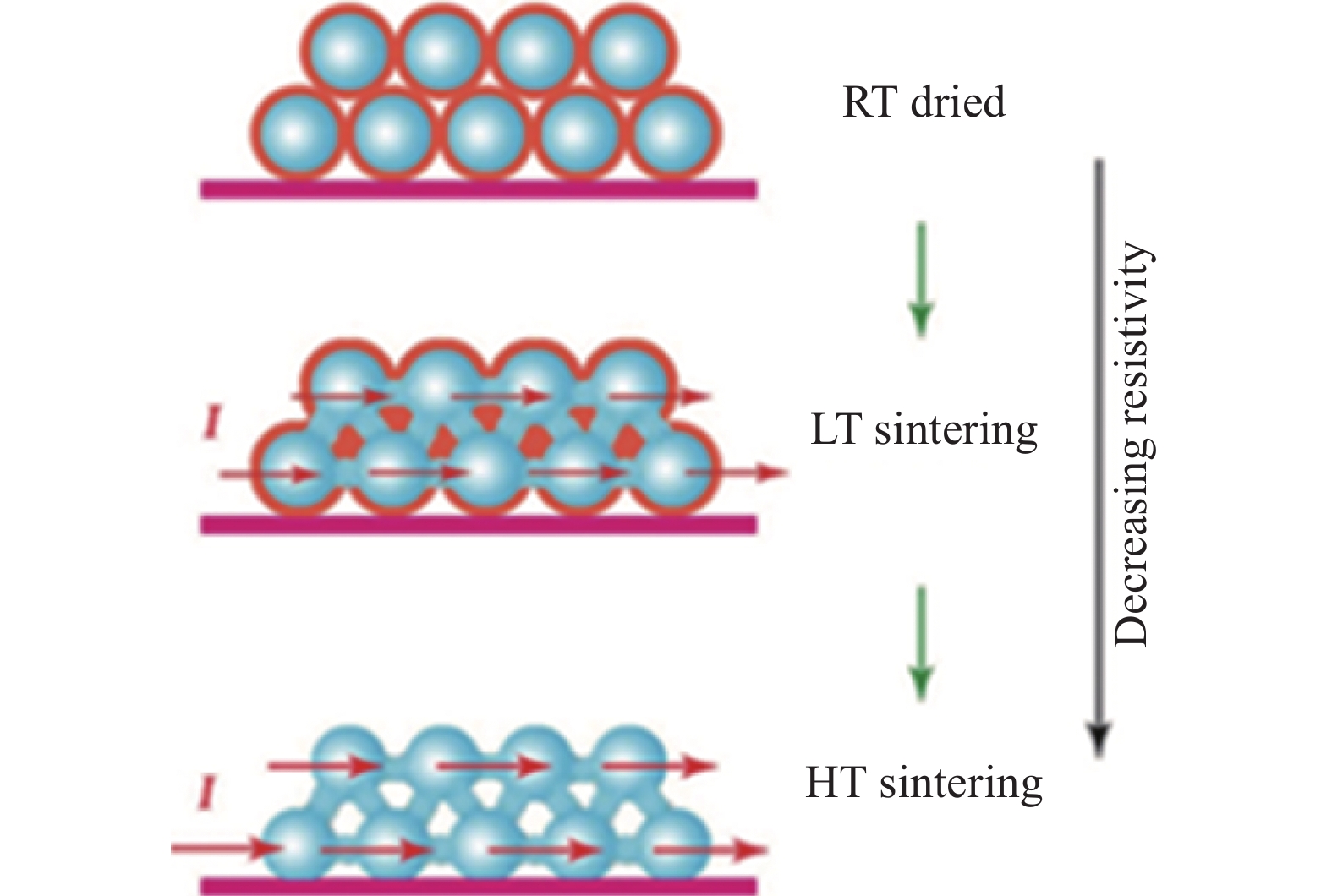
图 3 热烧结工艺示意图(RT表示室温,LT表示低温,HT表示高温)[56]
Figure 3. Schematic diagram of the thermal sintering process (RT indicates room temperature, LT indicates low temperature, and HT indicates high temperature)
![]()
![]()
![]()
表 1 不同前驱体纳米铜基导电油墨工艺、方法和稳定性
Table 1 Processes, methods and stability of copper nanobased conductive inks with different precursors
前驱体 基板 印刷—烧结方法 方阻/电阻率 温度—时间 参考文献 铜@银纳米颗粒 玻璃 丝网印刷—热烧结 113 mΩ·sq−1 室温—三周 [31] 铜@银纳米颗粒 玻璃 旋转丝网印刷—热烧结 0.60 Ω·sq−1 室温-两个月 [32] 铜@银纳米颗粒 聚酰亚胺(PI) 喷墨打印—热烧结 3.21 μΩ·cm 156 ℃-40 d [28] 铜@银纳米颗粒 玻璃 喷墨打印—热烧结 11 μΩ·cm NA [33] 铜@银纳米颗粒 玻璃 平面丝网印刷—热烧结 0.18 Ω·sq−1 室温-六个月 [34] 铜@银纳米颗粒 PI 旋转丝网印刷—激光烧结 28.5 μΩ·cm NA [35] 铜@银纳米颗粒 玻璃 旋转丝网印刷—热烧结 13.7 μΩ·cm NA [36] 铜@银纳米线 聚氨基甲酸酯(PU) 喷墨打印—热烧结 35 Ω·sq−1 140 ℃-500 h [37] 铜@金纳米线 玻璃 NA—热烧结 35 Ω·sq−1 80 ℃-700 h [38] 氧化铜纳米颗粒 PI NA—激光烧结 31 μΩ·cm NA [30] 氧化铜纳米颗粒 玻璃 旋转丝网印刷—激光烧结 9.5 μΩ·cm NA [39] 氧化铜纳米颗粒 聚乙烯(PE) 喷墨打印—强脉冲光烧结 3.1 μΩ·cm NA [40] 氧化铜纳米颗粒 聚对苯二甲酸乙二醇酯(PET) 喷墨打印—强脉冲光烧结 9 μΩ·cm NA [41]  下载: 导出CSV
-
[1] Lee H B, Bae C W, Duy L T, et al. Mogul-patterned elastomeric substrate for stretchable electronics[J]. Advanced Materials, 2016, 28(16): 3069 − 3077. doi: 10.1002/adma.201505218
[2] Wang Z, Xing R, Yu X, et al. Adhesive lithography for fabricating organic electronic and optoelectronics devices[J]. Nanoscale, 2011, 3(7): 2663 − 2678. doi: 10.1039/c1nr10039d
[3] Chen C W, Kang H W, Hsiao S Y, et al. Efficient and uniform planar-type perovskite solar cells by simple sequential vacuum deposition[J]. Advanced Materials, 2014, 26(38): 6647 − 6652. doi: 10.1002/adma.201402461
[4] Parashkov R, Becker E, Riedl T, et al. Large area electronics using printing methods[J]. Proceedings of the IEEE, 2005, 93(7): 1321 − 1329. doi: 10.1109/JPROC.2005.850304
[5] Cai J, Zhang C, Khan A, et al. Selective electroless metallization of micro-and nanopatterns via poly (dopamine) modification and palladium nanoparticle catalysis for flexible and stretchable electronic applications[J]. ACS applied materials & interfaces, 2018, 10(34): 28754 − 28763.
[6] Li J, Zhang X, Liu X, et al. Conductivity and foldability enhancement of Ag patterns formed by PVAc modified Ag complex inks with low-temperature and rapid sintering[J]. Materials & Design, 2020, 185: 108255.
[7] Cui Z. Printed electronics: materials, technologies and applications[M]. New Jersey: John Wiley & Sons, 2016.
[8] Nguyen P Q M, Yeo L P, Lok B K, et al. Patterned surface with controllable wettability for inkjet printing of flexible printed electronics[J]. ACS Applied Materials and Interfaces, 2014, 6(6): 4011 − 4016. doi: 10.1021/am4054546
[9] Nathan A, Ahnood A, Cole M T, et al. Flexible electronics: the next ubiquitous platform[J]. Proceedings of the IEEE, 2012, 100(Special Centennial Issue): 1486-1517.
[10] Magdassi S, Grouchko M, Kamyshny A. Copper nanoparticles for printed electronics: routes towards achieving oxidation stability[J]. Materials, 2010, 3(9): 4626 − 4638. doi: 10.3390/ma3094626
[11] 姜皎洁, 刘文涛, 黄灵阁, 等. 无线射频识别技术用导电油墨的研究[J]. 材料导报, 2015, 29(1): 121 − 126. doi: 10.11896/j.issn.1005-023X.2015.01.021 Jiang Jiaojie, Liu Wentao, Huang Lingge, et al. Research on conductive inks for radio frequency identification technology[J]. Materials Guide, 2015, 29(1): 121 − 126. doi: 10.11896/j.issn.1005-023X.2015.01.021
[12] 李金焕, 陆建辉, 王玉丰, 等. 金属银导电油墨的研究进展[J]. 电子元件与材料, 2014, 33(11): 14 − 17. doi: 10.14106/j.cnki.1001-2028.2014.11.004 Li Jinhuan, Lu Jianhui, Wang Yufeng, et al. Research progress of metallic silver conductive inks[J]. Electronic Components and Materials, 2014, 33(11): 14 − 17. doi: 10.14106/j.cnki.1001-2028.2014.11.004
[13] Bacalzo N P, Go L P, Querebillo C J, et al. Controlled microwave-hydrolyzed starch as a stabilizer for green formulation of aqueous gold nanoparticle ink for flexible printed electronics[J]. ACS Applied Nano Materials, 2018, 1(3): 1247 − 1256. doi: 10.1021/acsanm.7b00379
[14] Liu X, Kanehara M, Liu C, et al. Spontaneous patterning of high-resolution electronics via parallel vacuum ultraviolet[J]. Advanced Materials, 2016, 28(31): 6568 − 6573. doi: 10.1002/adma.201506151
[15] Guo Rumeng, Xiao Yubo, Gao Ye et al. Interfacial enhancement of Ag and Cu particles sintering using(111)-oriented nanotwinned Cu as substrate for die-attachment[J]. China Welding, 2022, 31(1): 22 − 28.
[16] Wang X, Guo W, Zhu Y, et al. Electrical and mechanical properties of ink printed composite electrodes on plastic substrates[J]. Applied Sciences, 2018, 8(11): 2101. doi: 10.3390/app8112101
[17] Stempien Z, Rybicki T, Rybicki E, et al. In-situ deposition of polyaniline and polypyrrole electroconductive layers on textile surfaces by the reactive ink-jet printing technique[J]. Synthetic Metals, 2015, 202: 49 − 62. doi: 10.1016/j.synthmet.2015.01.027
[18] Zhao P, Zhang R, Tong Y, et al. All-paper, all-organic, cuttable, and foldable pressure sensor with tuneable conductivity polypyrrole[J]. Advanced Electronic Materials, 2020, 6(8): 1 − 10.
[19] Htwe Y Z N, Mariatti M. Surfactant-assisted water-based graphene conductive inks for flexible electronic applications[J]. Journal of the Taiwan Institute of Chemical Engineers, 2021, 125: 402 − 412. doi: 10.1016/j.jtice.2021.06.022
[20] Aziz A, Bazbouz M B, Welland M E. Double-walled carbon nanotubes ink for high-conductivity flexible electrodes[J]. ACS Applied Nano Materials, 2020, 3(9): 9385 − 9392. doi: 10.1021/acsanm.0c02013
[21] 杨婉春, 王帅, 祝温泊, 等. 低温烧结纳米铜焊膏的制备及其连接性能分析[J]. 焊接学报, 2018, 39(6): 72 − 76. doi: 10.12073/j.hjxb.2018390152 Yang Wanchun, Wang Shuai, Zhu Wenbo, et al. Preparation of low-temperature sintered nano-copper solder paste and its connection performance analysis[J]. Transactions of the China Welding Institution, 2018, 39(6): 72 − 76. doi: 10.12073/j.hjxb.2018390152
[22] Nie X, Wang H, Zou J. Inkjet printing of silver citrate conductive ink on PET substrate[J]. Applied Surface Science, 2012, 261: 554 − 560. doi: 10.1016/j.apsusc.2012.08.054
[23] 奚甡. 中外银矿资源现状分析[J]. 世界有色金属, 2012, 6: 60 − 63. Xi Shen. Analysis of the current situation of silver resources in China and abroad[J]. World Non-ferrous Metals, 2012, 6: 60 − 63.
[24] 罗晓玲. 国内外铜矿资源分析[J]. 世界有色金属, 2000, 4(4): 4 − 10. Luo Xiaoling. Analysis of domestic and foreign copper ore resources[J]. World Non-ferrous Metals, 2000, 4(4): 4 − 10.
[25] Zhou X, Guo W, Zhu Y, et al. The laser writing of highly conductive and anti-oxidative copper structures in liquid[J]. Nanoscale, 2020, 12(2): 563 − 571. doi: 10.1039/C9NR07248A
[26] Chen H, Lee J H, Kim Y H, et al. Metallic copper nanostructures synthesized by a facile hydrothermal method[J]. Journal of Nanoscience and Nanotechnology, 2010, 10(1): 629 − 636. doi: 10.1166/jnn.2010.1739
[27] Zhang B, Li W, Jiu J, et al. Large-scale and galvanic replacement free synthesis of Cu@Ag core-shell nanowires for flexible electronics[J]. Inorganic Chemistry, 2019, 58(5): 3374 − 3381. doi: 10.1021/acs.inorgchem.8b03460
[28] Zhang W, Zhou Y, Ding Y, et al. Sintering mechanism of size-controllable Cu-Ag core-shell nanoparticles for flexible conductive film with high conductivity, antioxidation, and electrochemical migration resistance[J]. Applied Surface Science, 2022, 586: 152691. doi: 10.1016/j.apsusc.2022.152691
[29] Zhao J, Zhang D, Zhang X. Preparation and characterization of copper/silver bimetallic nanowires with core-shell structure[J]. Surface and Interface Analysis, 2015, 47(4): 529 − 534. doi: 10.1002/sia.5743
[30] Kang B, Han S, Kim J, et al. One-step fabrication of copper electrode by laser-induced direct local reduction and agglomeration of copper oxide nanoparticle[J]. The Journal of Physical Chemistry C, 2011, 115(48): 23664 − 23670. doi: 10.1021/jp205281a
[31] Yu X, Li J, Shi T, et al. A green approach of synthesizing of Cu-Ag core-shell nanoparticles and their sintering behavior for printed electronics[J]. Journal of Alloys and Compounds, 2017, 724: 365 − 372. doi: 10.1016/j.jallcom.2017.07.045
[32] Lee C, Kim N R, Koo J, et al. Cu-Ag core-shell nanoparticles with enhanced oxidation stability for printed electronics[J]. Nanotechnology, 2015, 26(45): 455601. doi: 10.1088/0957-4484/26/45/455601
[33] Grouchko M, Kamyshny A, Magdassi S. Formation of air-stable copper-silver core-shell nanoparticles for inkjet printing[J]. Journal of Materials Chemistry, 2009, 19(19): 3057 − 3062. doi: 10.1039/b821327e
[34] Pajor-Świerzy A, Farraj Y, Kamyshny A, et al. Air stable copper-silver core-shell submicron particles: Synthesis and conductive ink formulation[J]. Colloids and Surfaces A:Physicochemical and Engineering Aspects, 2017, 521: 272 − 280.
[35] Titkov A I, Logutenko O A, Vorobyev A M, et al. Laser sintering of Cu@Ag core-shell nanoparticles for printed electronics applications[J]. Materials Today:Proceedings, 2020, 25: 447 − 450. doi: 10.1016/j.matpr.2019.12.163
[36] Kim N R, Lee Y J, Lee C, et al. Surface modification of oleylamine-capped Ag-Cu nanoparticles to fabricate low-temperature-sinterable Ag-Cu nanoink[J]. Nanotechnology, 2016, 27(34): 345706. doi: 10.1088/0957-4484/27/34/345706
[37] Zhang B, Li W, Nogi M, et al. Alloying and embedding of Cu-core/Ag-shell nanowires for ultrastable stretchable and transparent electrodes[J]. ACS Applied Materials & Interfaces, 2019, 11(20): 18540 − 18547.
[38] Niu Z, Cui F, Yu Y, et al. Ultrathin epitaxial Cu@Au core-shell nanowires for stable transparent conductors[J]. Journal of the American Chemical Society, 2017, 139(21): 7348 − 7354. doi: 10.1021/jacs.7b02884
[39] Rahman M K, Lu Z, Kwon K S. Green laser sintering of copper oxide (CuO) nano particle (NP) film to form Cu conductive lines[J]. AIP Advances, 2018, 8(9): 095008. doi: 10.1063/1.5047562
[40] Öhlund T, Schuppert A K, Hummelgard M, et al. Inkjet fabrication of copper patterns for flexible electronics: using paper with active precoatings[J]. ACS Applied Materials & Interfaces, 2015, 7(33): 18273 − 18282.
[41] Paquet C, James R, Kell A J, et al. Photosintering and electrical performance of CuO nanoparticle inks[J]. Organic Electronics, 2014, 15(8): 1836 − 1842. doi: 10.1016/j.orgel.2014.05.014
[42] Zhang B, Li W, Jiu J, et al. Large-scale and galvanic replacement free synthesis of Cu@Ag core-shell nanowires for flexible electronics[J]. Inorganic Chemistry, 2019, 58(5): 3374 − 3381. doi: 10.1021/acs.inorgchem.8b03460
[43] Dai X, Xu W, Zhang T, et al. Room temperature sintering of Cu-Ag core-shell nanoparticles conductive inks for printed electronics[J]. Chemical Engineering Journal, 2019, 364: 310 − 319. doi: 10.1016/j.cej.2019.01.186
[44] Draper G L, Dharmadasa R, Staats M E, et al. Fabrication of elemental copper by intense pulsed light processing of a copper nitrate hydroxide ink[J]. ACS Applied Materials & Interfaces, 2015, 7(30): 16478 − 16485.
[45] Son S G, Park H J, Kim Y K, et al. Fabrication of low-cost and flexible potassium ion sensors based on screen printing and their electrochemical characteristics[J]. Applied Chemistry for Engineering, 2019, 30(6): 737 − 741.
[46] Lee H, Lee D, Hwang J, et al. Silver nanoparticle piezoresistive sensors fabricated by roll-to-roll slot-die coating and laser direct writing[J]. Optics Express, 2014, 22(8): 8919 − 8927. doi: 10.1364/OE.22.008919
[47] Zhu D, Wang Z, Zhu D. Highly conductive graphene electronics by inkjet printing[J]. Journal of Electronic Materials, 2020, 49(3): 1765 − 1776. doi: 10.1007/s11664-019-07920-1
[48] Secor E B, Lim S, Zhang H, et al. Gravure printing of graphene for large-area flexible electronics[J]. Advanced Materials, 2014, 26(26): 4533 − 4538. doi: 10.1002/adma.201401052
[49] Lau P H, Takei K, Wang C, et al. Fully printed, high performance carbon nanotube thin-film transistors on flexible substrates[J]. Nano Letters, 2013, 13(8): 3864 − 3869. doi: 10.1021/nl401934a
[50] Mariappan D D. Nanoporous flexographic printing: fundamentals, applications and scale-up[D]. Massachusetts Institute of Technology, 2019.
[51] Søndergaard R R, Hösel M, Krebs F C. Roll-to-Roll fabrication of large area functional organic materials[J]. Journal of Polymer Science, Part B:Polymer Physics, 2013, 51(1): 16 − 34. doi: 10.1002/polb.23192
[52] Singh M, Haverinen H M, Dhagat P, et al. Inkjet printing-process and its applications[J]. Advanced Materials, 2010, 22(6): 673 − 685. doi: 10.1002/adma.200901141
[53] Khan S, Doh Y H, Khan A, et al. Direct patterning and electrospray deposition through EHD for fabrication of printed thin film transistors[J]. Current Applied Physics, 2011, 11(1): S271 − S279. doi: 10.1016/j.cap.2010.11.044
[54] Gu Y, Wu A, Federici J F, et al. Inkjet printable constantan ink for the fabrication of flexible and conductive film[J]. Chemical Engineering Journal, 2017, 313: 27 − 36. doi: 10.1016/j.cej.2016.12.071
[55] Choi Y, Seong K, Piao Y. Metal-organic decomposition ink for printed electronics[J]. Advanced Materials Interfaces, 2019, 6(20): 1901002. doi: 10.1002/admi.201901002
[56] Sugiyama T, Kanzaki M, Arakawa R, et al. Low-temperature sintering of metallacyclic stabilized copper nanoparticles and adhesion enhancement of conductive copper film to a polyimide substrate[J]. Journal of Materials Science:Materials in Electronics, 2016, 27(7): 7540 − 7547. doi: 10.1007/s10854-016-4734-8
[57] 李俊龙, 徐杨, 赵雪龙, 等. 铜颗粒低温烧结技术的研究进展[J]. 焊接学报, 2022, 43(3): 13 − 24. doi: 10.12073/j.hjxb.20210225002 Li Junlong, Xu Yang, Zhao Xuelong, et al. Research progress of low-temperature sintering technology for copper particles[J]. Transactions of the China Welding Institution, 2022, 43(3): 13 − 24. doi: 10.12073/j.hjxb.20210225002
[58] Kim I, Kim J. The effect of reduction atmospheres on the sintering behaviors of inkjet-printed Cu interconnectors[J]. Journal of Applied Physics, 2010, 108(10): 102807. doi: 10.1063/1.3511688
[59] Gu W, Yuan W, Zhong T, et al. Fast near infrared sintering of silver nanoparticle ink and applications for flexible hybrid circuits[J]. RSC Advances, 2018, 8(53): 30215 − 30222. doi: 10.1039/C8RA04468F
[60] Park B K, Kim D, Jeong S, et al. Direct writing of copper conductive patterns by ink-jet printing[J]. Thin solid films, 2007, 515(19): 7706 − 7711. doi: 10.1016/j.tsf.2006.11.142
[61] Zhai D, Zhang T, Guo J, et al. Water-based ultraviolet curable conductive inkjet ink containing silver nano-colloids for flexible electronics[J]. Colloids and Surfaces A:Physicochemical and Engineering Aspects, 2013, 424: 1 − 9.
[62] MacNeill W, Choi C-H, Chang C-H, et al. On the self-damping nature of densification in photonic sintering of nanoparticles[J]. Scientific Reports, 2015, 5(1): 1 − 13. doi: 10.9734/JSRR/2015/14076
[63] Ryu C H, Joo S J, Kim H S. Intense pulsed light sintering of Cu nano particles/micro particles-ink assisted with heating and vacuum holding of substrate for warpage free printed electronic circuit[J]. Thin Solid Films, 2019, 675: 23 − 33. doi: 10.1016/j.tsf.2019.02.020
[64] Kim H S, Dhage S R, Shim D E, et al. Intense pulsed light sintering of copper nanoink for printed electronics[J]. Applied Physics A, 2009, 97(4): 791 − 798. doi: 10.1007/s00339-009-5360-6
[65] Öhlund T, Schuppert A K, Hummelgard M, et al. Inkjet fabrication of copper patterns for flexible electronics: using paper with active precoatings[J]. ACS Applied Materials & Interfaces, 2015, 7(33): 18273 − 18282.
[66] Wang B Y, Yoo T H, Song Y W, et al. Cu ion ink for a flexible substrate and highly conductive patterning by intensive pulsed light sintering[J]. ACS Applied Materials & Interfaces, 2013, 5(10): 4113 − 4119.
[67] Chung W H, Hwang H J, Kim H S. Flash light sintered copper precursor/nanoparticle pattern with high electrical conductivity and low porosity for printed electronics[J]. Thin Solid Films, 2015, 580: 61 − 70. doi: 10.1016/j.tsf.2015.03.004
[68] Paglia F, Vak D, Van Embden J, et al. Photonic sintering of copper through the controlled reduction of printed CuO nanocrystals[J]. ACS Applied Materials & Interfaces, 2015, 7(45): 25473 − 25478.
[69] Yu J H, Kang K T, Hwang J Y, et al. Rapid sintering of copper nano ink using a laser in air[J]. International Journal of Precision Engineering and Manufacturing, 2014, 15(6): 1051 − 1054. doi: 10.1007/s12541-014-0435-5
[70] 周兴汶, 廖嘉宁, 姚煜, 等. 铜微纳结构的激光直写及其应用研究进展[J]. 中国激光, 2021, 48(8): 141 − 153. Zhou Xingwen, Liao Jianing, Yao Yi, et al. Progress of laser direct writing of copper micro-nano structures and its application[J]. China Laser, 2021, 48(8): 141 − 153.
[71] Kang B, Han S, Kim J, et al. One-step fabrication of copper electrode by laser-induced direct local reduction and agglomeration of copper oxide nanoparticle[J]. The Journal of Physical Chemistry C, 2011, 115(48): 23664 − 23670. doi: 10.1021/jp205281a
[72] Ohishi T, Takahashi N. Preparation and properties of copper fine wire on polyimide film in air by laser irradiation and mixed-copper-complex solution containing glyoxylic acid copper complex and methylamine copper complex[J]. Materials Sciences and Applications, 2018, 9(11): 859. doi: 10.4236/msa.2018.911062
[73] Zhou X, Guo W, Fu J, et al. Laser writing of Cu/CuxO integrated structure on flexible substrate for humidity sensing[J]. Applied Surface Science, 2019, 494: 684 − 690. doi: 10.1016/j.apsusc.2019.07.159
[74] Kim K S, Bang J O, Choa Y H, et al. The characteristics of Cu nanopaste sintered by atmospheric-pressure plasma[J]. Microelectronic Engineering, 2013, 107: 121 − 124. doi: 10.1016/j.mee.2012.08.019
[75] Gao Y, Zhang H, Jiu J, et al. Fabrication of a flexible copper pattern based on a sub-micro copper paste by a low temperature plasma technique[J]. RSC Advances, 2015, 5(109): 90202 − 90208. doi: 10.1039/C5RA18583A
[76] Shi L, Layani M, Cai X, et al. An inkjet printed Ag electrode fabricated on plastic substrate with a chemical sintering approach for the electrochemical sensing of hydrogen peroxide[J]. Sensors and Actuators B:Chemical, 2018, 256: 938 − 945. doi: 10.1016/j.snb.2017.10.035
[77] Li D, Sutton D, Burgess A, et al. Conductive copper and nickel lines via reactive inkjet printing[J]. Journal of Materials Chemistry, 2009, 19(22): 3719 − 3724. doi: 10.1039/b820459d
[78] Li W, Zhang H, Gao Y, et al. Highly reliable and highly conductive submicron Cu particle patterns fabricated by low temperature heat-welding and subsequent flash light sinter-reinforcement[J]. Journal of Materials Chemistry C, 2017, 5(5): 1155 − 1164. doi: 10.1039/C6TC04892G
[79] Liao J, Guo W, Peng P. Direct laser writing of copper-graphene composites for flexible electronics[J]. Optics and Lasers in Engineering, 2021, 142: 106605. doi: 10.1016/j.optlaseng.2021.106605
[80] Walia S, Mondal I, Kulkarni G U. Patterned Cu-Mesh-based transparent and wearable touch panel for tactile, proximity, pressure, and temperature sensing[J]. ACS Applied Electronic Materials, 2019, 1(8): 1597 − 1604. doi: 10.1021/acsaelm.9b00330
[81] Zhou X, Guo W, Yao Y, et al. Flexible nonenzymatic glucose sensing with one-step laser-fabricated Cu2O/Cu porous structure[J]. Advanced Engineering Materials, 2021, 23(6): 2100192. doi: 10.1002/adem.202100192
[82] Yao Y, Guo W, Zhou X, et al. Thermal properties of laser-fabricated copper-carbon composite films on polyimide substrate[J]. Advanced Engineering Materials, 2021: 2100623.
[83] Peng Z, Lin J, Ye R, et al. Flexible and stackable laser-induced graphene supercapacitors[J]. ACS Applied Materials & Interfaces, 2015, 7(5): 3414 − 3419.
[84] Liu H, Liu Y, Guo W, et al. Laser assisted ink-printing of copper oxide nanoplates for memory device[J]. Materials Letters, 2020, 261: 127097. doi: 10.1016/j.matlet.2019.127097
-
期刊类型引用(6)
1. 严蓬辉,陈绪兵,彭伊丽,谢发东. 基于改进YOLOv5s的激光软钎焊焊点缺陷检测算法. 激光与光电子学进展. 2024(08): 219-228 .  百度学术
百度学术
2. 张丽娜. 基于三角激光的机械臂构件缺陷检测方法研究. 激光杂志. 2024(04): 233-237 . 百度学术
3. 迟大钊,王梓明,刘海春,李庆生,郭强,苏维刚,贾涛. 基于超声TOFD法B扫描图像预测的缺陷定位. 焊接学报. 2024(12): 1-6 . 本站查看
4. 刘茂. 激光超声检测技术在管道壁厚及焊接缺陷检测中的应用研究. 现代制造技术与装备. 2022(04): 136-138 . 百度学术
5. 石颖颖,赵金玲,杨乐辉,赵建平. 含分层复合材料管道中超声导波的模态转换特性研究. 压力容器. 2022(03): 81-88 . 百度学术
6. 李建宾,石拓,傅戈雁,王明雨,王宇,李天奕,刘广. 基于激光内送粉的十字交叉结构熔覆成形工艺研究. 光学学报. 2022(16): 168-174 . 百度学术
其他类型引用(3)


计量
- 文章访问数: 230
- HTML全文浏览量: 121
- PDF下载量: 22
- 被引次数: 9
