
Research progress of low-temperature Cu-Cu bonding technology for advanced packaging
-
摘要: Cu-Cu低温键合技术是先进封装的核心技术,相较于目前主流应用的Sn基软钎焊工艺,其互连节距更窄、导电导热能力更强、可靠性更优. 文中对应用于先进封装领域的Cu-Cu低温键合技术进行了综述,首先从工艺流程、连接机理、性能表征等方面较系统地总结了热压工艺、混合键合工艺实现Cu-Cu低温键合的研究进展与存在问题,进一步地阐述了新型纳米材料烧结工艺在实现低温连接、降低工艺要求方面的优越性,概述了纳米线、纳米多孔骨架、纳米颗粒初步实现可图形化的Cu-Cu低温键合基本原理. 结果表明,基于纳米材料烧结连接的基本原理,继续开发出宽工艺冗余、窄节距图形化、优良互连性能的Cu-Cu低温键合技术是未来先进封装的重要发展方向之一.Abstract: Low-temperature Cu-Cu bonding technology is the core technology for advanced packaging. Compared with the mainstream Sn-based soldering process, it can achieve finer pitch, higher electrical and thermal conductivity. In this paper, low-temperature Cu-Cu bonding technology for advanced packaging is reviewed. The research progress of low-temperature Cu-Cu bonding realized by thermal compression bonding and hybrid bonding is systematically summarized from the aspects of process flow, bonding mechanism and performance characterization. The advantages of the newly-developed nanomaterial sintering process in reducing bonding temperature and process requirements are further expounded. Mechanism of patterned nanowires, nano-porous frameworks and nanoparticles for low-temperature bonding are summarized. Low-temperature Cu-Cu bonding technology for advanced packaging are forecast.
-
Keywords:
- advanced packaging /
- hybrid bonding /
- Cu-Cu bonding /
- fine pitch /
- sintering
-
-
![]()
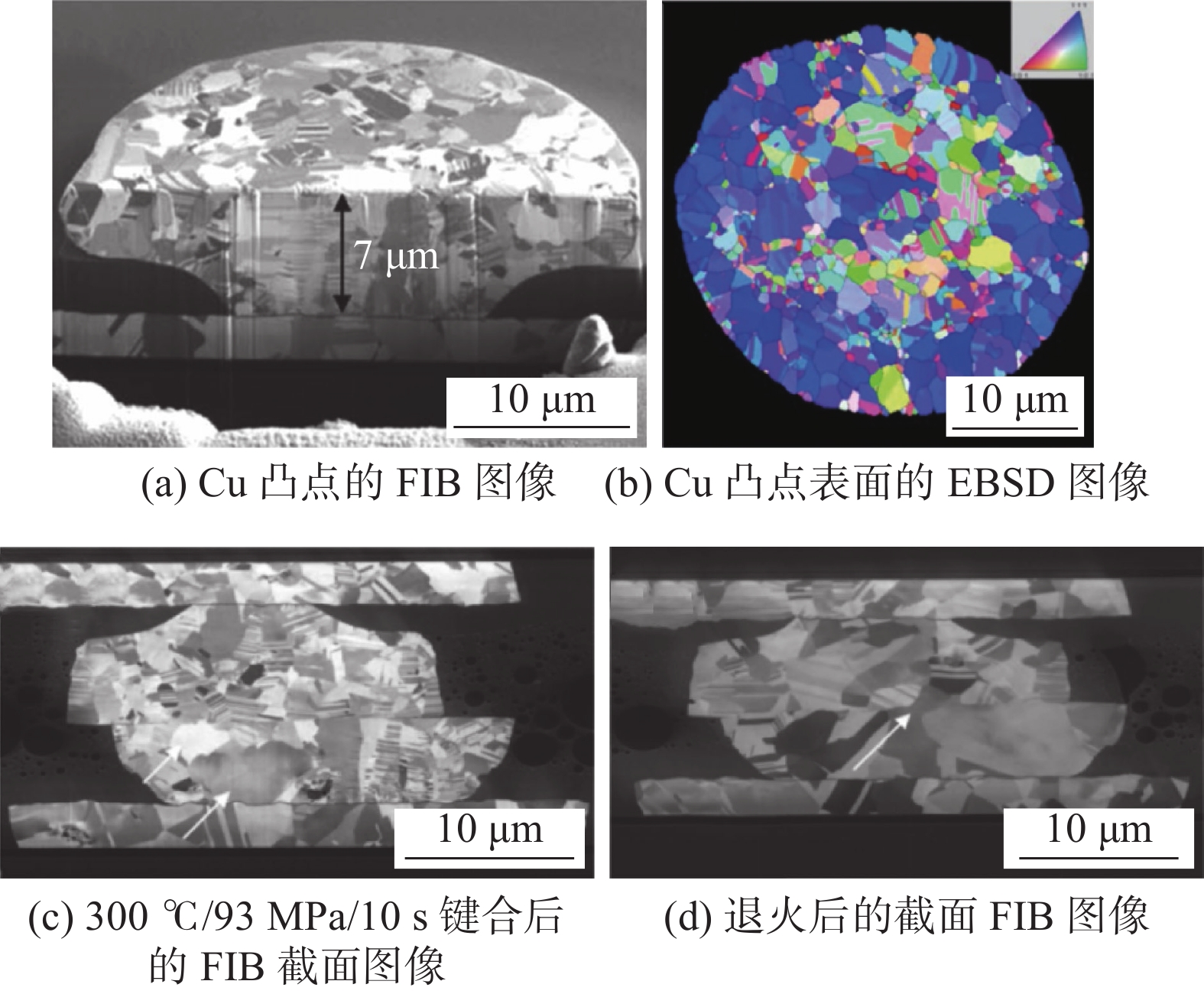
图 1 由(111) 取向的纳米孪晶Cu凸点实现Cu-Cu键合[15-17]
Figure 1. Cu-Cu bonding enabled by (111)-oriented nanotwinned Cu bumps. (a) The microbump cross-section analyzed by FIB; (b) surface orientation of an nt-Cu microbump observed by EBSD; (c) cross-sectional FIB ion-image of a Cu joint bonded at 300 ℃/93 MPa/10 s; (d) cross-sectional FIB ion-image for post-annealed sample
![]()
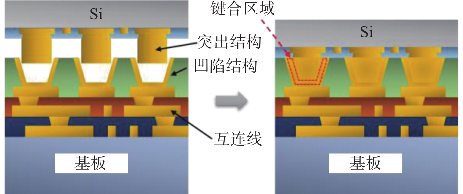
图 2 飞行切割[19]
Figure 2. Fly-cutting. (a) schematic illustration of fly-cutting; (b) optical images of cut Cu bumps surface
![]()
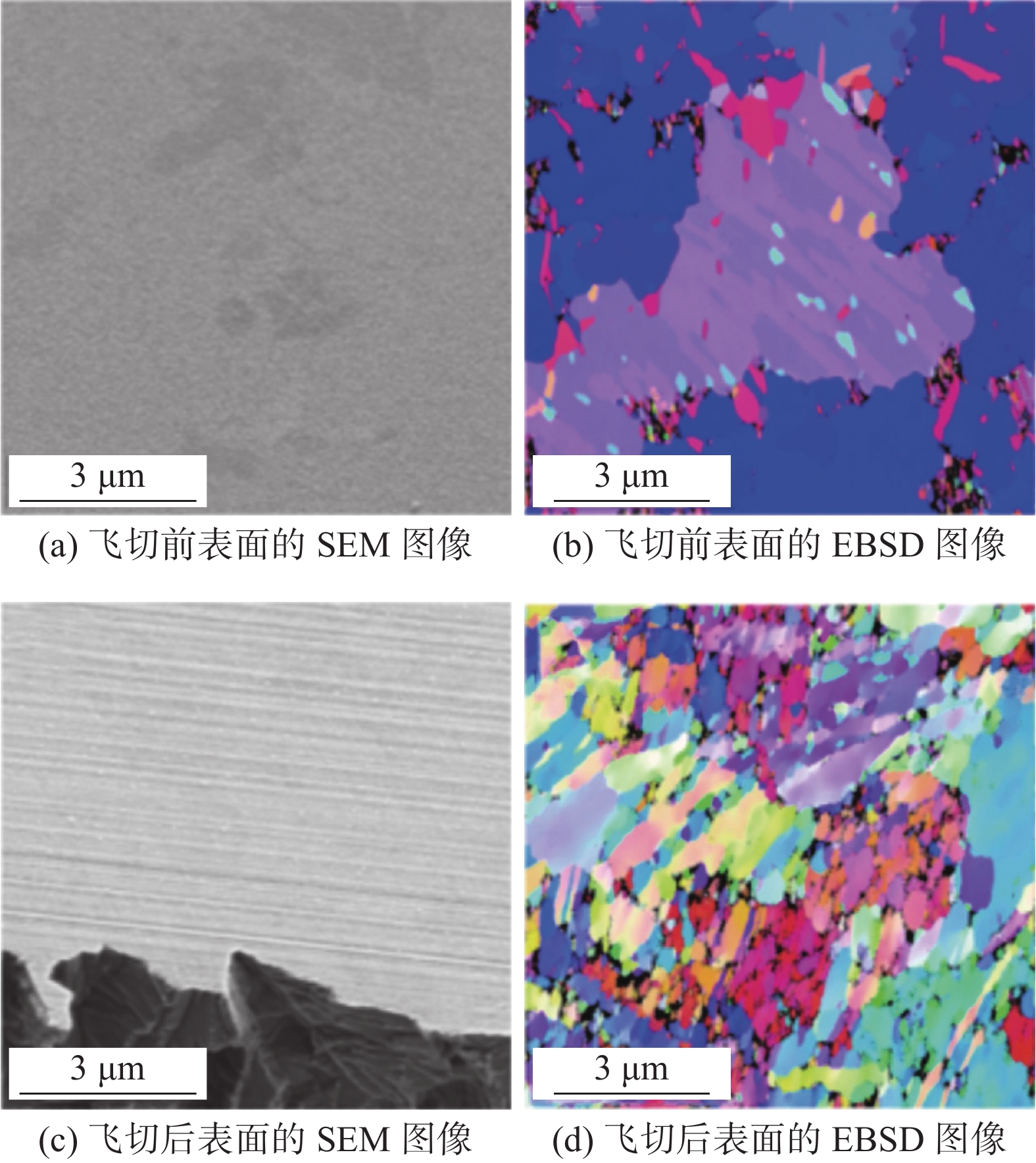
图 3 飞行切割细化表面晶粒[20]
Figure 3. Fly-cutting process introduces finer grains. (a) SEM image of initial Cu surface; (b) EBSD image of initial Cu surface; (c) SEM image of cut Cu surface; (d) EBSD image of cut Cu surface
![]()
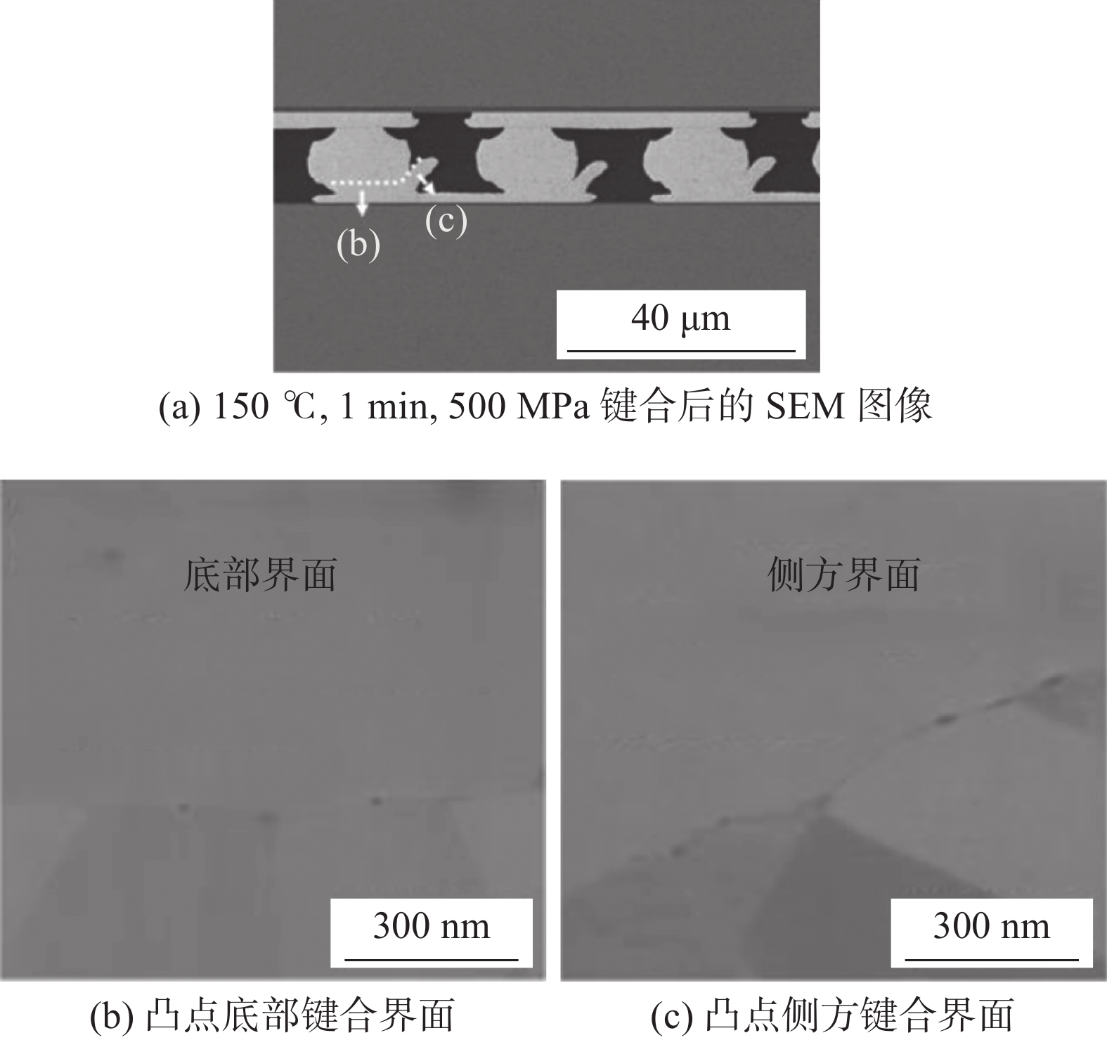
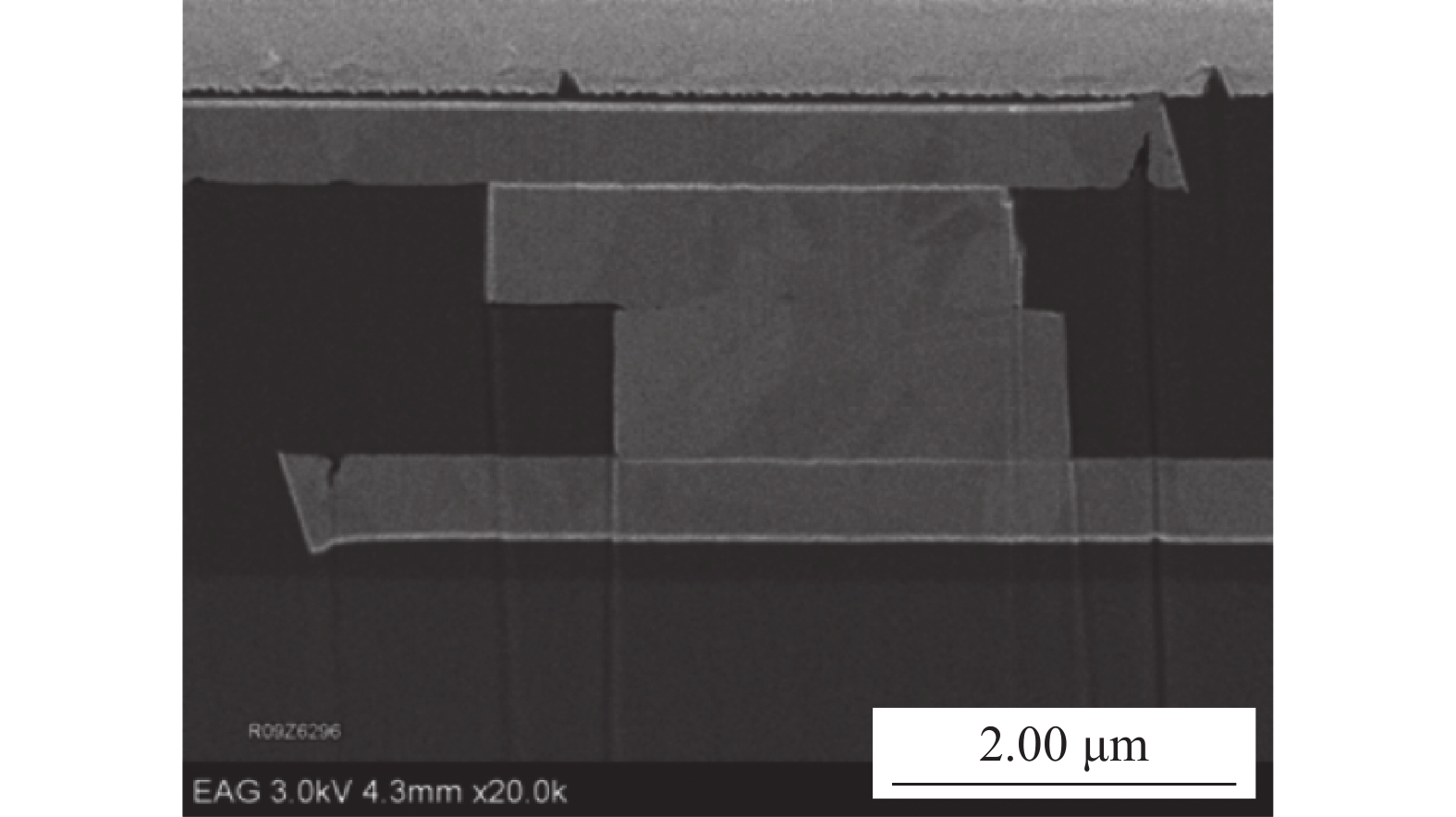
图 5 键合后的SEM图像[22]
Figure 5. SEM cross-sectional view of Cu-Cu bonding. (a) with bonding condition of 150 ℃, 1 min, 500 MPa; (b) bottom bonding interface; (c) sidewall bonding interface
![]()
![]()
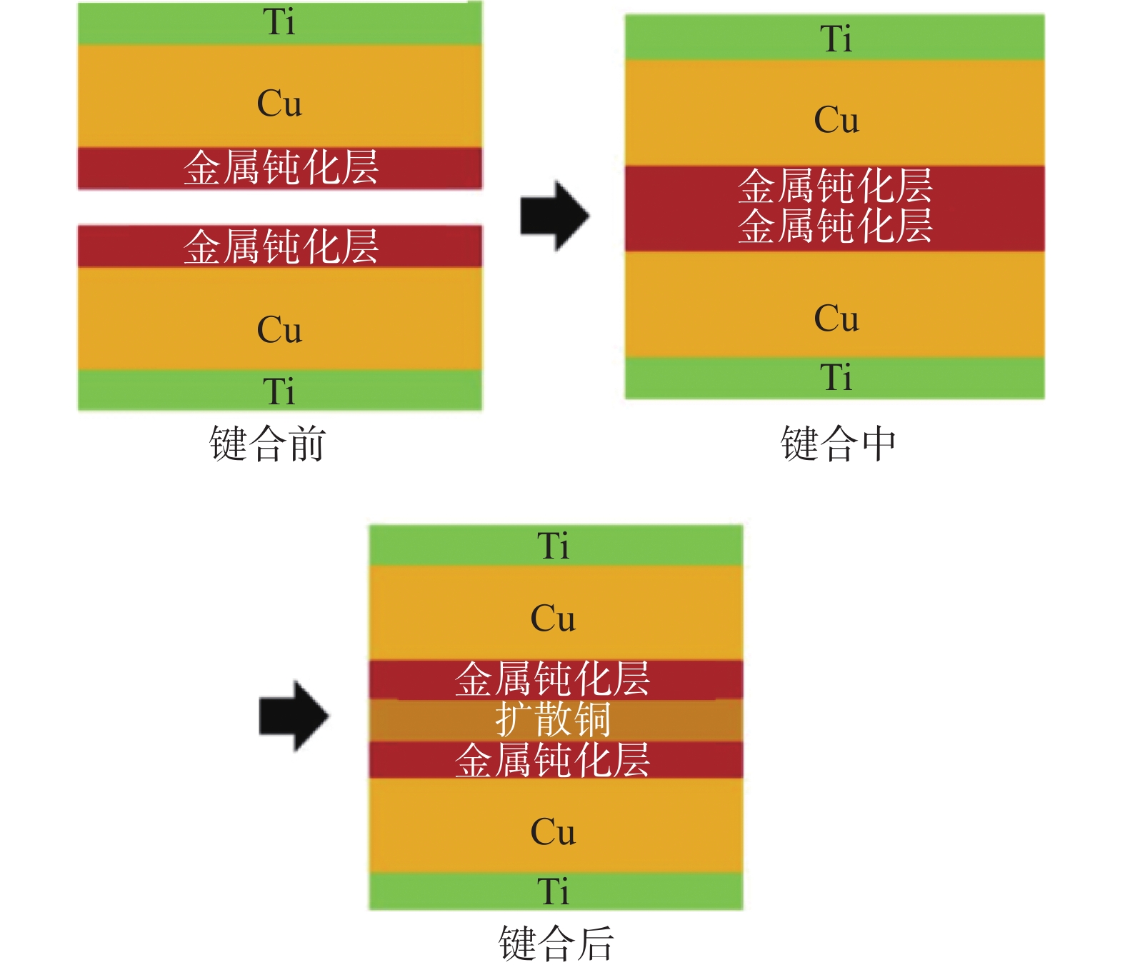
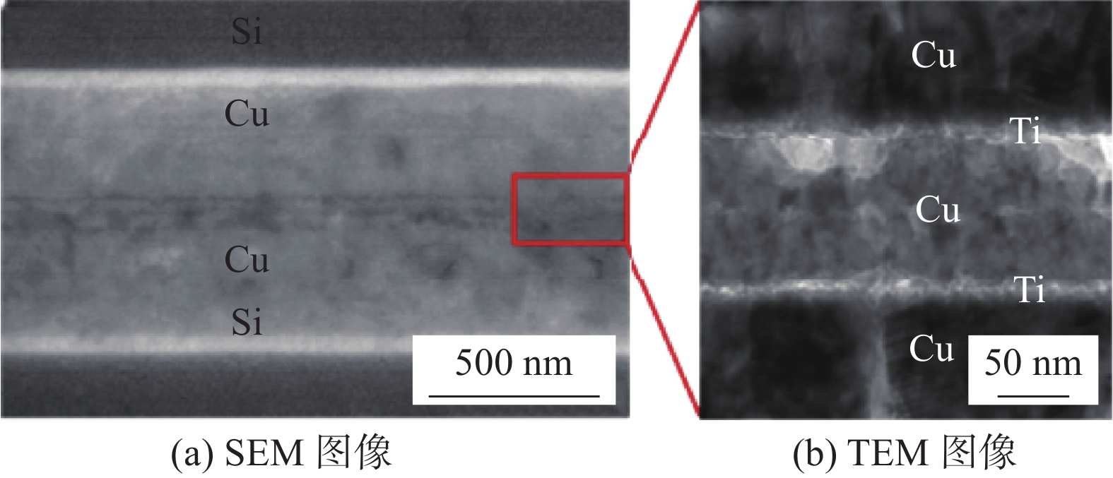
图 8 Ti作钝化层的键合结果[26]
Figure 8. Ti passivation bonded results. (a) SEM image; (b) TEM image
![]()
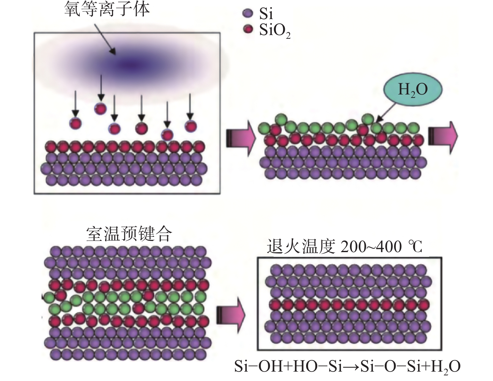
图 9 自组装分子层钝化方法的原理和工艺流程[31]
Figure 9. Schematic illustration and process flow of self-assembled monolayer method. (a) before bonding; (b) after bonding
![]()
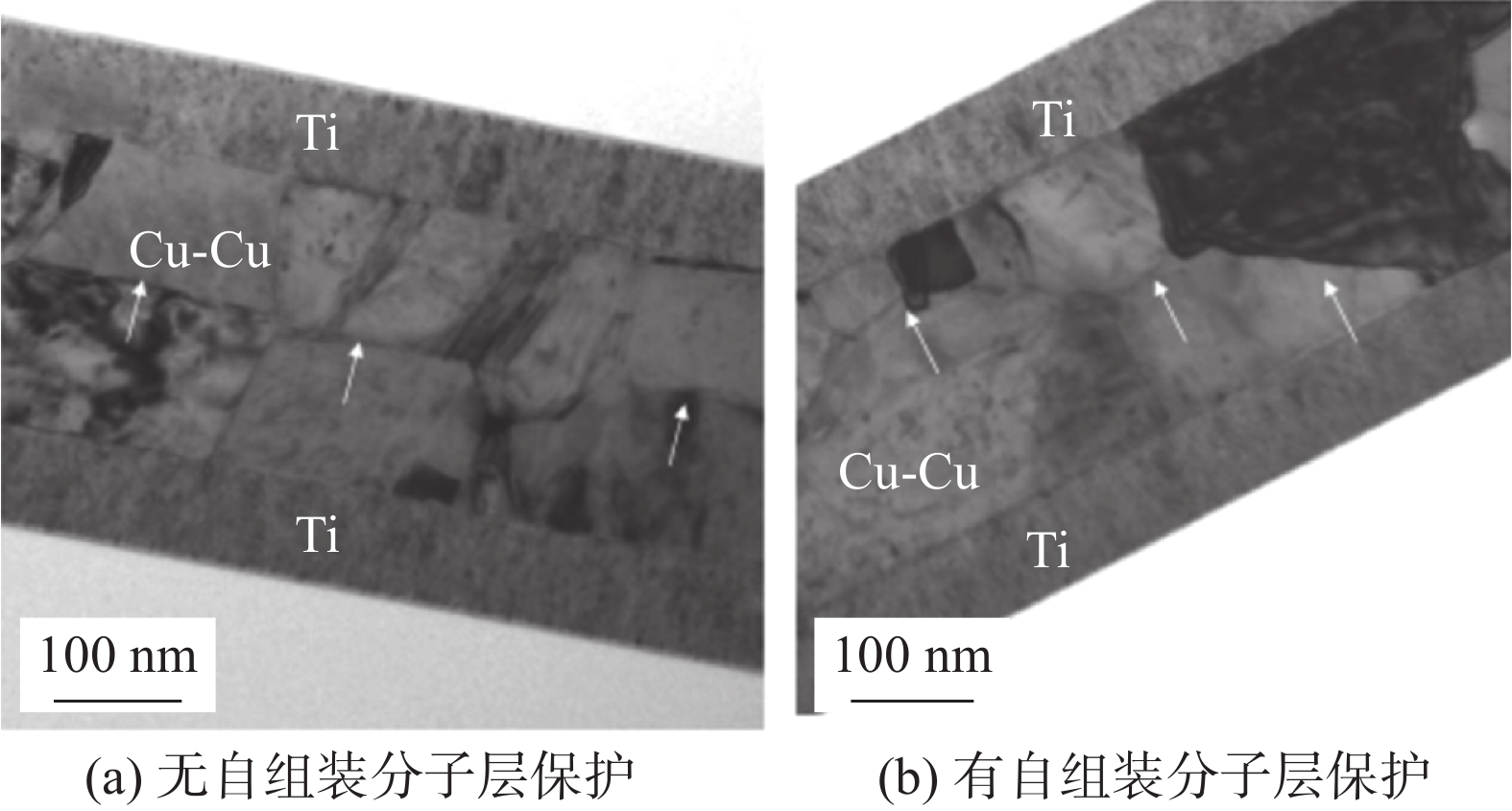
图 10 Cu-Cu键合界面的TEM图像[32]
Figure 10. TEM micrographs of bonded Cu layers. (a) without SAM passivation; (b) with SAM passivation
![]()
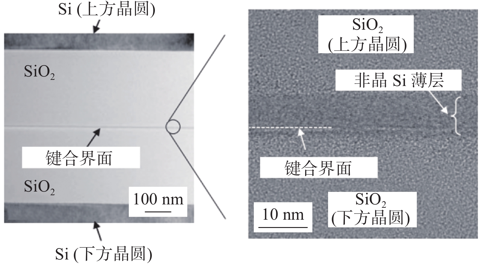
图 14 Si作为SiO2-SiO2室温键合的中间层[44]
Figure 14. Bonding of SiO2 and SiO2 at room temperature using Si ultrathin film
![]()
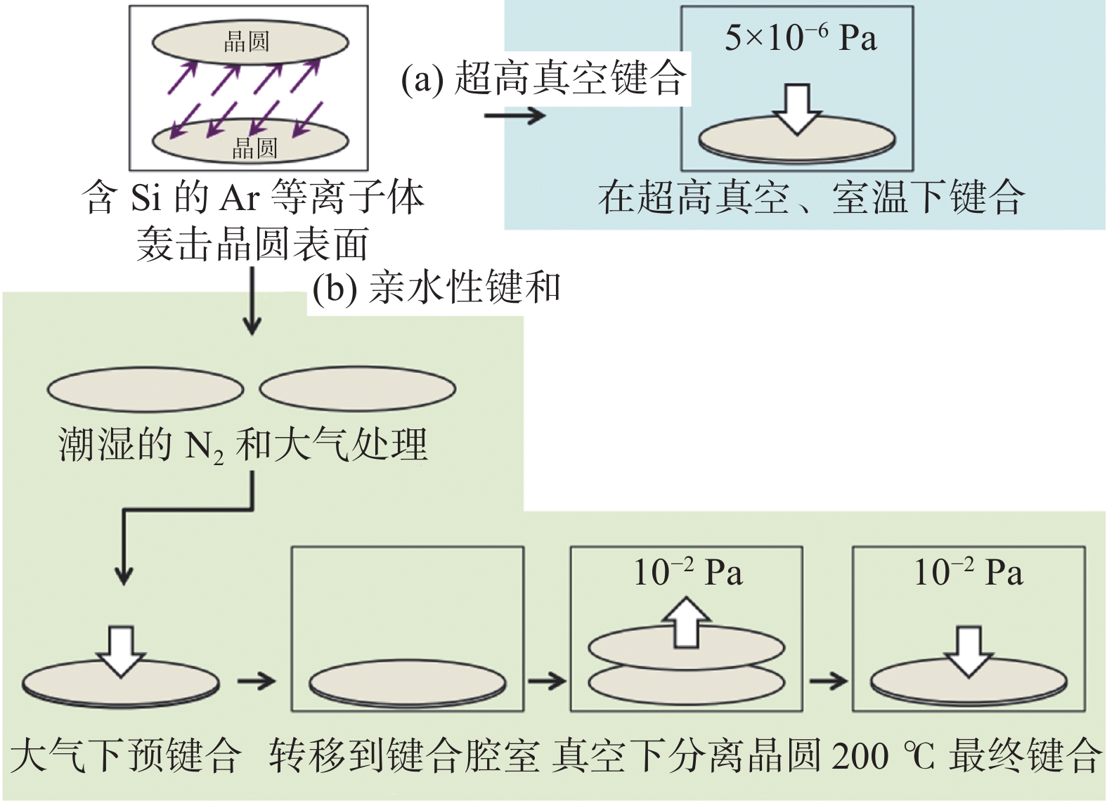
图 15 基于SAB的混合键合流程示意图[46]
Figure 15. Process flow of the combined SAB with (a) UHV bonding and (b) hydrophilic bonding
![]()
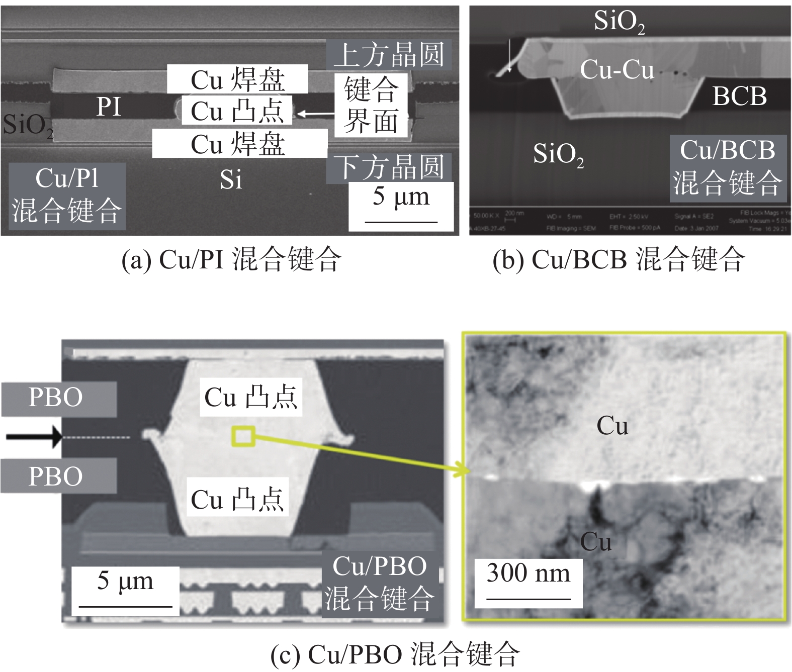
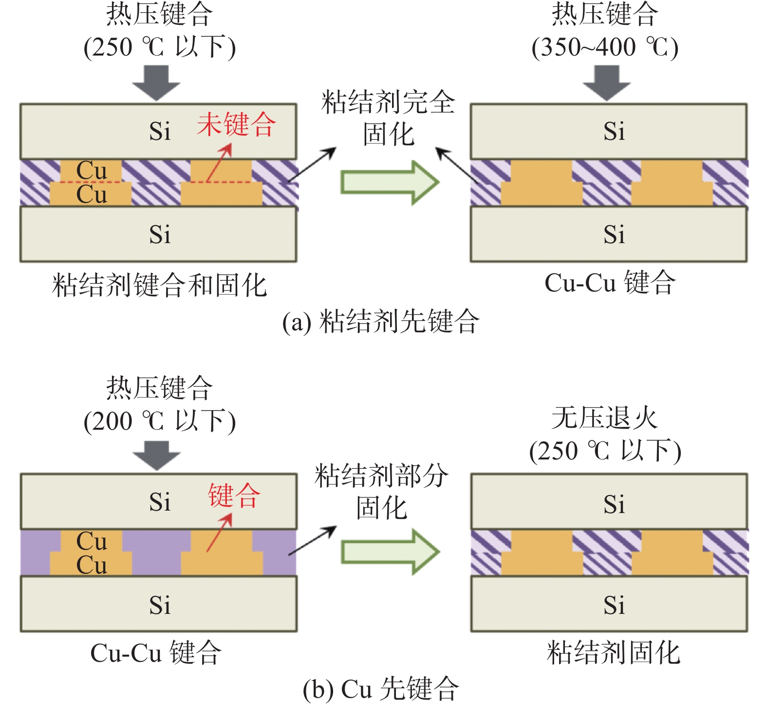
图 17 Cu和粘结剂混合键合方式[50]
Figure 17. Cu/adhesive hybrid bonding. (a) “adhesive-first” hybrid bonding process; (b) “Cu-first” hybrid bonding process
![]()
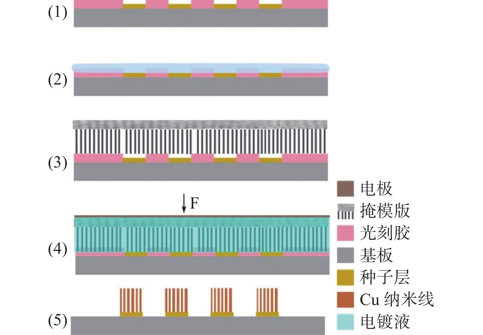
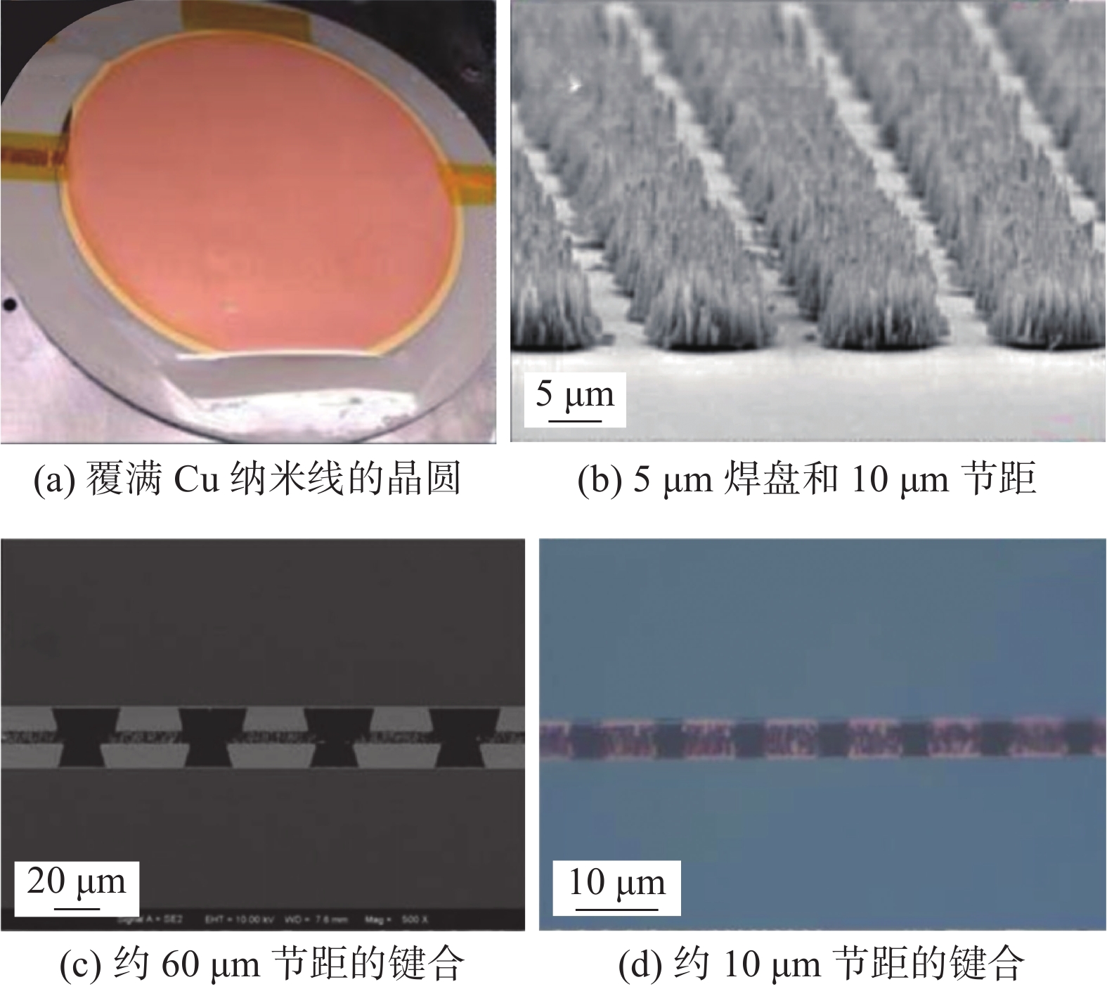
图 19 键合前后的Cu纳米线[56]
Figure 19. Cu nanowires before and after bonding. (a) entire wafer covered with Cu nanowires; (b) 5 μm pads with 10 μm pitch; (c) cross sections of about 60 μm and; (d) 10 μm pitch connected with nanowires
![]()
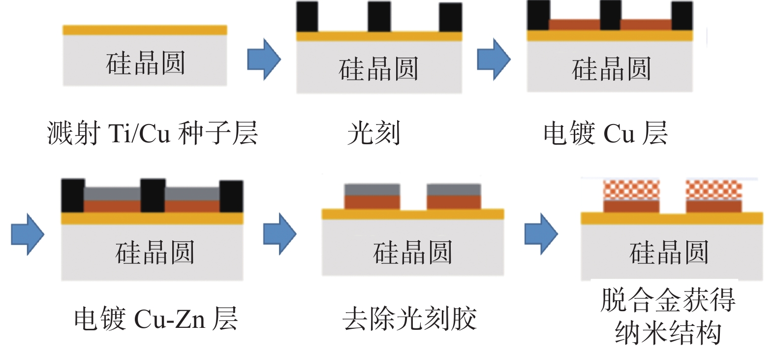
图 20 Cu纳米多孔骨架的图形化路线[62]
Figure 20. Process flow for fabrication of patterned np-Cu foam films
![]()
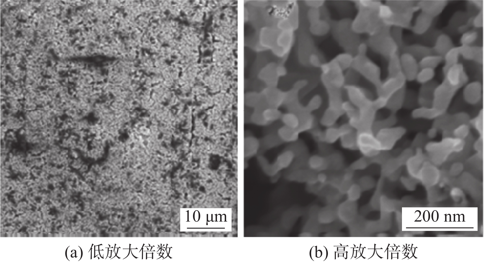
图 21 纳米多孔骨架的组织形态[62]
Figure 21. Morphology of dealloyed np-Cu foam film. (a) low magnification; (b) high magnification
![]()
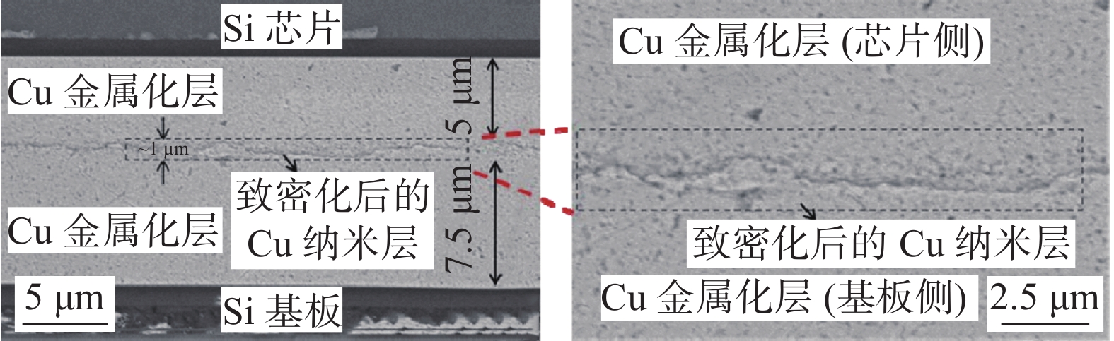
图 22 250 ℃/9 MPa/30 min烧结条件下的键合界面[62]
Figure 22. Cross-sectional images of the sintered joint under the condition of 250 ℃/9 MPa/30 min
![]()
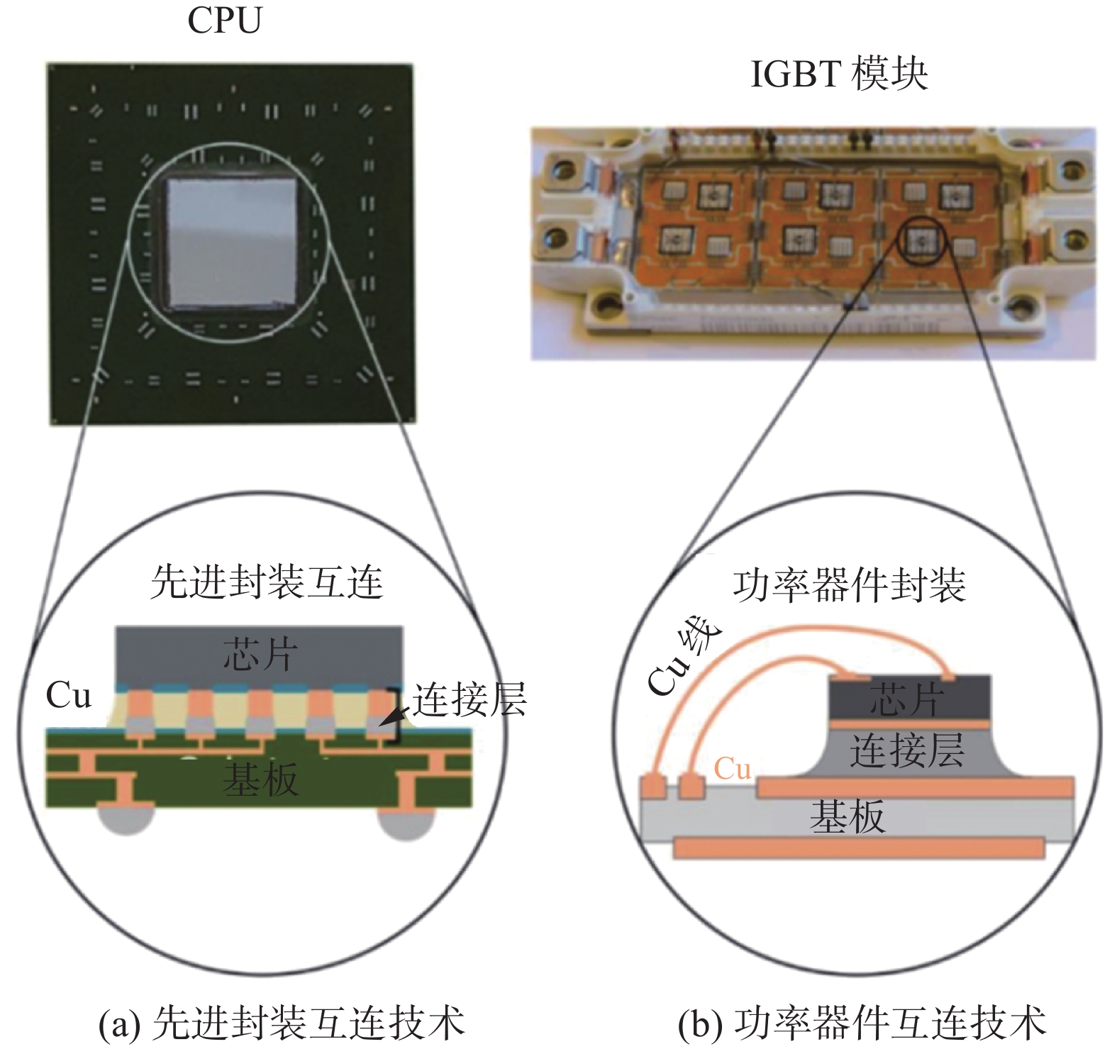
图 23 不同互连技术的示意图[67]
Figure 23. Schematic of different packaging technology. (a) advanced packaging technology; (b) power device packaging technology
![]()
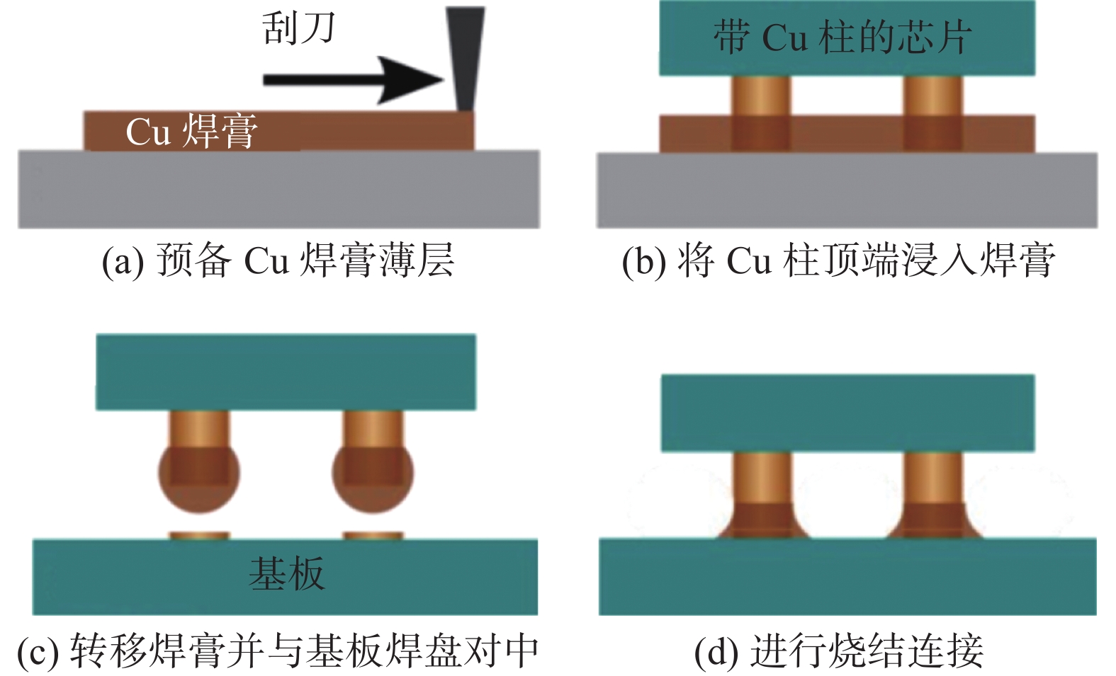
图 24 浸蘸转移法进行焊膏图形化[68]
Figure 24. Process sequence of the dipping method. (a) preparation of a Cu ink film; (b) dip into Cu ink film by Cu pillar chip; (c) ink transfer and alignment to substrate; (d) joint formed by nanoparticle sintering
![]()
图 25 键合压力对接头组织和剪切强度的影响[71]
Figure 25. Effects of bonding pressure on microstructures and interconnect resistance. (a) microstructures; (b) interconnect resistance
-
[1] Moore G E. Cramming more components onto integrated circuits[J]. Proceedings of the IEEE, 1998, 86(1): 82 − 85. doi: 10.1109/JPROC.1998.658762
[2] Waldrop M M. The chips are down for Moore’s law[J]. Nature News, 2016, 530(7589): 144. doi: 10.1038/530144a
[3] Li Y, Goyal D. Introduction to 3D microelectronic packaging[M]. 3D Microelectronic Packaging, Springer, 2021.
[4] Shahane N M. Reliable fine-pitch chip-to-substrate copper interconnections with high-through assembly and high power-handling[D]. Georgia Institute of Technology, 2018.
[5] Miller L F. Controlled collapse reflow chip joining[J]. IBM Journal of Research and Development, 1969, 13(3): 239 − 250. doi: 10.1147/rd.133.0239
[6] Kim J M, Shin Y E, Fujimoto K. Dynamic modeling for resin self-alignment mechanism[J]. Microelectronics Reliability, 2004, 44(6): 983 − 992. doi: 10.1016/j.microrel.2004.01.006
[7] Fang M, Tang C, Chen Y, et al. Thermo-compression bonding process characteristics and shape control of Cu-pillar microbump joints by optimizing of solder melting[J]. Journal of Materials Science: Materials in Electronics, 2022, 33(13): 10471 − 10485. doi: 10.1007/s10854-022-08034-x
[8] Zhang L, Ou S, Huang J, et al. Effect of current crowding on void propagation at the interface between intermetallic compound and solder in flip chip solder joints[J]. Applied Physics Letters, 2006, 88(1): 012106. doi: 10.1063/1.2158702
[9] Wang S, Hsu L, Wang N, et al. EBSD investigation of Cu-Sn IMC microstructural evolution in Cu/Sn-Ag/Cu microbumps during isothermal annealing[J]. Journal of Electronic Materials, 2014, 43(1): 219 − 228. doi: 10.1007/s11664-013-2675-z
[10] Chen K N, Fan A, Tan C, et al. Bonding parameters of blanket copper wafer bonding[J]. Journal of Electronic Materials, 2006, 35(2): 230 − 234. doi: 10.1007/BF02692440
[11] Chen K N, Fan A, Reif R. Microstructure examination of copper wafer bonding[J]. Journal of Electronic Materials, 2001, 30(4): 331 − 335. doi: 10.1007/s11664-001-0039-6
[12] Chen K N, Tan C S, Fan A, et al. Morphology and bond strength of copper wafer bonding[J]. Electrochemical and Solid-State Letters, 2004, 7(1): G14. doi: 10.1149/1.1626994
[13] Grayson A C R, Cima M J, Langer R. Size and temperature effects on poly (lactic-co-glycolic acid) degradation and microreservoir device performance[J]. Biomaterials, 2005, 26(14): 2137 − 2145. doi: 10.1016/j.biomaterials.2004.06.033
[14] Juang J Y, Lu C L, Chen K J, et al. Copper-to-copper direct bonding on highly (111)-oriented nanotwinned copper in no-vacuum ambient[J]. Scientific Reports, 2018, 8(1): 13910. doi: 10.1038/s41598-018-32280-x
[15] Juang J Y, Lu C L, Li Y J, et al. A solid state process to obtain high mechanical strength in Cu-to-Cu joints by surface creep on (111)-oriented nanotwins Cu[J]. Journal of Materials Research and Technology, 2021, 14: 719 − 730. doi: 10.1016/j.jmrt.2021.06.099
[16] Shie K C, Juang J Y, Chen C. Instant Cu-to-Cu direct bonding enabled by (111)-oriented nanotwinned Cu bumps[J]. Japanese Journal of Applied Physics, 2020, 59(SB): SBBA03. doi: 10.7567/1347-4065/ab5697
[17] Ong J J, Shie K C, Tu K N, et al. Two-step fabrication process for die-to-die and die-to-wafer Cu-Cu bonds[C]//2021 IEEE 71th Electronic Components and Technology Conference (ECTC), 2021: 203 − 210.
[18] Liu C M, Lin H W, Huang Y S, et al. Low-temperature direct copper-to-copper bonding enabled by creep on (111) surfaces of nanotwinned Cu[J]. Scientific Reports, 2015, 5(1): 1 − 11. doi: 10.9734/JSRR/2015/14076
[19] Sakai T, Imaizumi N, Miyajima T. Low temperature Cu-Cu direct bonding for 3D-IC by using fine crystal layer[C]//2012 2nd IEEE Transactions on Components, Packaging and Manufacturing Technology Symposium Japan, 2012: 1 − 4.
[20] Al Farisi M S, Hirano H, Tanaka S. Low-temperature hermetic thermo-compression bonding using electroplated copper sealing frame planarized by fly-cutting for wafer-level MEMS packaging[J]. Sensors and Actuators A: Physical, 2018, 279: 671 − 679. doi: 10.1016/j.sna.2018.06.021
[21] Yang Y T, Chou T C, Yu T Y, et al. Low-temperature Cu-Cu direct bonding using pillar–concave structure in advanced 3-D heterogeneous integration[J]. IEEE Transactions on Components, Packaging and Manufacturing Technology, 2017, 7(9): 1560 − 1566. doi: 10.1109/TCPMT.2017.2720468
[22] Chou T C, Yang K M, Li J C, et al. Investigation of pillar–concave structure for low-temperature Cu–Cu direct bonding in 3D/2.5D heterogeneous integration[J]. IEEE Transactions on Components, Packaging and Manufacturing Technology, 2020, 10(8): 1296 − 1303. doi: 10.1109/TCPMT.2020.3004969
[23] Takagi H, Kikuchi K, Maeda R, et al. Surface activated bonding of silicon wafers at room temperature[J]. Applied Physics Letters, 1996, 68(16): 2222 − 2224. doi: 10.1063/1.115865
[24] Suga T, Mu F. Surface activated bonding method for low temperature bonding[C]// 2018 7th Electronic System-Integration Technology Conference (ESTC), 2018: 1 − 4.
[25] Shigetou A, Itoh T, Sawada K, et al. Bumpless interconnect of 6-μm-pitch Cu electrodes at room temperature[J]. IEEE Transactions on Advanced Packaging, 2008, 31(3): 473 − 478. doi: 10.1109/TADVP.2008.920644
[26] Huang Y P, Chien Y S, Tzeng R N, et al. Novel Cu-to-Cu bonding with Ti passivation at 180 ℃ in 3D integration[J]. IEEE Electron Device Letters, 2013, 34(12): 1551 − 1553. doi: 10.1109/LED.2013.2285702
[27] Panigrahi A K, Bonam S, Ghosh T, et al. Ultra-thin Ti passivation mediated breakthrough in high quality Cu-Cu bonding at low temperature and pressure[J]. Materials Letters, 2016, 169: 269 − 272. doi: 10.1016/j.matlet.2016.01.126
[28] Liu D, Chen P C, Chou T C, et al. Demonstration of low-temperature fine-pitch Cu/SiO hybrid bonding by Au passivation[J]. IEEE Journal of the Electron Devices Society, 2021, 9: 868 − 875. doi: 10.1109/JEDS.2021.3114648
[29] Chou T C, Huang S Y, Chen P J, et al. Electrical and reliability investigation of Cu-to-Cu bonding with silver passivation layer in 3D integration[J]. IEEE Transactions on Components, Packaging and Manufacturing Technology, 2020, 11(1): 36 − 42.
[30] Hong Z J, Liu D, Hu H W, et al. Ultra-High strength Cu-Cu bonding under low thermal budget for chiplet heterogeneous applications[C]// 2021 IEEE 71st Electronic Components and Technology Conference (ECTC), 2021: 347 − 352.
[31] Peng L, Zhang L, Fan J, et al. Ultrafine pitch (6 μm) of recessed and bonded Cu–Cu interconnects by three-dimensional wafer stacking[J]. IEEE Electron Device Letters, 2012, 33(12): 1747 − 1749. doi: 10.1109/LED.2012.2218273
[32] Tan C S, Lim D F, Singh S G, et al. Cu–Cu diffusion bonding enhancement at low temperature by surface passivation using self-assembled monolayer of alkane-thiol[J]. Applied Physics Letters, 2009, 95(19): 192108. doi: 10.1063/1.3263154
[33] Di Cioccio L, Gueguen P, Taibi R, et al. An overview of patterned metal/dielectric surface bonding: mechanism, alignment and characterization[J]. Journal of the Electrochemical Society, 2011, 158(6): 81. doi: 10.1149/1.3577596
[34] Moriceau H, Rieutord F, Fournel F, et al. Low temperature direct bonding: An attractive technique for heterostructures build-up[J]. Microelectronics Reliability, 2012, 52(2): 331 − 41. doi: 10.1016/j.microrel.2011.08.004
[35] Liang D, Fang A W, Park H, et al. Low-temperature, strong SiO2-SiO2 covalent wafer bonding for III–V compound semiconductors-to-silicon photonic integrated circuits[J]. Journal of Electronic Materials, 2008, 37(10): 1552 − 1559. doi: 10.1007/s11664-008-0489-1
[36] Baklanov M, Shamiryan D, Tökei Z, et al. Characterization of Cu surface cleaning by hydrogen plasma[J]. Journal of Vacuum Science & Technology B: Microelectronics and Nanometer Structures Processing, Measurement, and Phenomena, 2001, 19(4): 1201 − 1211.
[37] Écija D, Gallego J M, Miranda R. The adsorption of atomic N and the growth of copper nitrides on Cu (1 0 0)[J]. Surface Science, 2009, 603(15): 2283 − 2289. doi: 10.1016/j.susc.2009.04.039
[38] Ito F, Shobha H, Tagami M, et al. Effective Cu surface pre-treatment for high-reliable 22 nm-node Cu dual damascene interconnects with high plasma resistant ultra low-k dielectric (k= 2.2)[J]. Microelectronic Engineering, 2012, 92: 62 − 66. doi: 10.1016/j.mee.2011.01.077
[39] Park M, Baek S, Kim S, et al. Argon plasma treatment on Cu surface for Cu bonding in 3D integration and their characteristics[J]. Applied Surface Science, 2015, 324: 168 − 173. doi: 10.1016/j.apsusc.2014.10.098
[40] 王晨曦, 王特, 许继开, 等. 晶圆直接键合及室温键合技术研究进展[J]. 精密成形工程, 2018, 10(1): 67 − 73. doi: 10.3969/j.issn.1674-6457.2018.01.008 Wang Chenxi, Wang Te, Xu Jikai, et al. Research progress of wafer direct bonding and room-temperature bonding technology[J]. Journal of Netshape Forming Engineering, 2018, 10(1): 67 − 73. doi: 10.3969/j.issn.1674-6457.2018.01.008
[41] Ko C T, Chen K N. Low temperature bonding technology for 3D integration[J]. Microelectronics Reliability, 2012, 52(2): 302 − 311. doi: 10.1016/j.microrel.2011.03.038
[42] Enquist P, Fountain G, Petteway C, et al. Low cost of ownership scalable copper direct bond interconnect 3D IC technology for three dimensional integrated circuit applications[C]//2009 IEEE International Conference on 3D System Integration, 2009: 1 − 6.
[43] Gao G, Mirkarimi L, Workman T, et al. Development of low temperature direct bond interconnect technology for die-to-wafer and die-to-die applications-stacking, yield improvement, reliability assessment[C]//2018 IEEE International Wafer Level Packaging Conference (IWLPC), 2018: 1 − 7.
[44] Utsumi J, Ide K, Ichiyanagi Y. Bonding of SiO2 and SiO2 at room temperature using Si ultrathin film[J]. ECS Transactions, 2016, 75(9): 355 − 361. doi: 10.1149/07509.0355ecst
[45] Utsumi J, Ide K, Ichiyanagi Y. Cu/SiO2 hybrid bonding obtained by surface-activated bonding method at room temperature using Si ultrathin films[J]. Micro and Nano Engineering, 2019, 2: 1 − 6. doi: 10.1016/j.mne.2018.11.004
[46] He R, Fujino M, Yamauchi A, et al. Combined surface activated bonding technique for low-temperature Cu/dielectric hybrid bonding[J]. Journal of Solid State Science and Technology, 2016, 5(7): 419. doi: 10.1149/2.0201607jss
[47] Hsiao Z C, Ko C T, Chang H H, et al. Cu/BCB hybrid bonding with TSV for 3D integration by using fly cutting technology[C]// 2015 International Conference on Electronics Packaging and iMAPS All Asia Conference (ICEP-IAAC), 2015: 834 − 837.
[48] Takeda K, Aoki M. 3D integration technology using hybrid wafer bonding and via-last TSV process[C]// 2014 IEEE International Interconnect Technology Conference, 2014: 211 − 214.
[49] Yu R, Liu F, Polastre R, et al. Reliability of a 300-mm-compatible 3DI technology based on hybrid Cu-adhesive wafer bonding[C]//2009 Symposium on VLSI Technology, 2009: 170 − 171.
[50] He R, Fujino M, Akaike M, et al. Combined surface activated bonding using H-containing HCOOH vapor treatment for Cu/Adhesive hybrid bonding at below 200 °C[J]. Applied Surface Science, 2017, 414: 163 − 170. doi: 10.1016/j.apsusc.2017.03.168
[51] He R, Suga T. Effects of Ar plasma and Ar fast atom bombardment (FAB) treatments on Cu/polymer hybrid surface for wafer bonding[C]//2014 International Conference on Electronics Packaging (ICEP), 2014: 78 − 81.
[52] Kagawa Y, Fujii N, Aoyagi K, et al. Novel stacked CMOS image sensor with advanced Cu2Cu hybrid bonding[C]//2016 IEEE International Electron Devices Meeting (IEDM), 2016: 8.4.1 − 8.4.4.
[53] Buffat P, Borel J P. Size effect on the melting temperature of gold particles[J]. Physical Review A, 1976, 13(6): 2287 − 2298. doi: 10.1103/PhysRevA.13.2287
[54] Feng B, Shen D, Wang W, et al. Cooperative bilayer of lattice-disordered nanoparticles as room-temperature sinterable nanoarchitecture for device integrations[J]. ACS Applied Materials & Interfaces, 2019, 11(18): 16972 − 16980.
[55] Roustaie F, Quednau S, Dassinger F, et al. Room temperature interconnection technology for bonding fine pitch bumps using NanoWiring, KlettWelding, KlettSintering and KlettGlueing[C]//2020 15th International Microsystems, Packaging, Assembly and Circuits Technology Conference (IMPACT), 2020: 168 − 171.
[56] Roustaie F, Quednau S, Weissenborn F, et al. Room temperature KlettWelding interconnect technology for high performance CMOS logic[C]//2021 IEEE 71st Electronic Components and Technology Conference (ECTC), 2021: 371 − 376.
[57] Strahringer D, Roustaie F, Weissenborn F, et al. Optimizing the Nano Wiring and KlettSintering parameters for low-temperature die to DCB attach of power electronic chips[C]//2021 16th International Microsystems, Packaging, Assembly and Circuits Technology Conference (IMPACT), 2021: 31 − 34.
[58] Yu Z, Tan Y Z, Bayer C F, et al. Cu-Cu Thermocompression bonding with Cu-nanowire films for power semiconductor die-attach on DBC substrates[C]//2021 IEEE 23rd Electronics Packaging Technology Conference (EPTC), 2021: 1 − 7.
[59] Shahane N, Mohan K, Behera R, et al. Novel high-temperature, high-power handling all-Cu interconnections through low-temperature sintering of nanocopper foams[C]//2016 IEEE 66th Electronic Components and Technology Conference (ECTC), 2016: 829 − 836.
[60] Sosa R A, Mohan K, Antoniou A, et al. Low-temperature all-Cu interconnections formed by pressure-less sintering of Cu-pillars with nanoporous-Cu caps[C]//2021 IEEE 71st Electronic Components and Technology Conference (ECTC), 2021: 390 − 394.
[61] Shahane N, Mohan K, Ramos G, et al. Enabling chip-to-substrate all-Cu interconnections: design of engineered bonding interfaces for improved manufacturability and low-temperature bonding[C]//2017 IEEE 67th Electronic Components and Technology Conference (ECTC), 2017: 968 − 975.
[62] Mohan K, Shahane N, Sosa R A, et al. Demonstration of patternable all-Cu compliant interconnections with enhanced manufacturability in chip-to-substrate applications[C]//2018 IEEE 68th Electronic Components and Technology Conference (ECTC), 2018: 301 − 307.
[63] Sosa R A, Mohan K, Nguyen L, et al. Cu pillar with nanocopper caps: the next interconnection node beyond traditional Cu pillar[C]//2019 IEEE 69th Electronic Components and Technology Conference (ECTC), 2019: 655 − 660.
[64] Zhang B, Damian A, Zijl J, et al. In-air sintering of copper nanoparticle paste with pressure-assistance for die attachment in high power electronics[J]. Journal of Materials Science: Materials in Electronics, 2021, 32(4): 4544 − 4555. doi: 10.1007/s10854-020-05196-4
[65] 李俊龙, 徐杨, 赵雪龙, 等. 铜颗粒低温烧结技术的研究进展[J]. 焊接学报, 2022, 43(3): 13 − 24. Li Junlong, Xuyang, Zhao Xuelong, et al. Research progress of low temperature sintering technology for Cu particles[J]. Transactions of the China Welding Institution, 2022, 43(3): 13 − 24.
[66] Guo R, Xiao Y, Gao Y, et al. Interfacial enhancement of Ag and Cu particles sintering using (111)-oriented nanotwinned Cu as substrate for die-attachment[J]. China Welding, 2022, 31(1): 22 − 28.
[67] Del Carro L. Sintering of copper nanoparticle pastes for microelectronic packaging[D]. Swiss Federal Institute of Technology in Zurich, 2018.
[68] Del Carro L, Kossatz M, Schnackenberg L, et al. Laser sintering of dip-based all-copper interconnects[C]//2018 IEEE 68th Electronic Components and Technology Conference (ECTC), 2018: 279 − 286.
[69] Del Carro L, Zürcher J, Drechsler U, et al. Low-temperature dip-based all-copper interconnects formed by pressure-assisted sintering of copper nanoparticles[J]. IEEE Transactions on Components, Packaging and Manufacturing Technology, 2019, 9(8): 1613 − 1622. doi: 10.1109/TCPMT.2019.2891111
[70] Zürcher J, Yu K, Schlottig G, et al. Nanoparticle assembly and sintering towards all-copper flip chip interconnects[C]//2015 IEEE 65th Electronic Components and Technology Conference (ECTC), 2015: 1115 − 1121.
[71] Zürcher J, Del Carro L, Schlottig G, et al. All-copper flip chip interconnects by pressureless and low temperature nanoparticle sintering[C]//2016 IEEE 66th Electronic Components and Technology Conference (ECTC), 2016: 343 − 349.
[72] Mimatsu H, Mizuno J, Kasahara T, et al. Low-temperature gold-gold bonding using selective formation of nanoporous powders for bump interconnects[C]//2014 IEEE 27th International Conference on Micro Electro Mechanical Systems (MEMS), 2014: 1131 − 1134.
 下载:
下载:


计量
- 文章访问数: 1417
- HTML全文浏览量: 331
- PDF下载量: 327
