
Effect of wire current on microstructure and properties of 7075-T6 aluminum alloy joint welded by double-wire pulsed cold metal transition method
-
摘要: 为提高7075-T6铝合金熔化焊接接头性能,提出了一种双丝脉冲冷金属过渡(DW-CMTP)焊接方法,并研究了双丝平均电流大小对6 mm厚7075-T6铝合金对接接头组织和力学性能的影响. 结果表明,通过调控主、从丝电流可实现DW-CMTP焊接过程无明显飞溅且焊后接头成形效果良好;增加主、从丝平均电流分别能够促进熔深和熔宽;提高主丝平均电流可增大气泡上浮力,提高从丝平均电流则可加强熔池流动,以致均促进了焊缝中气体逸出,且从丝平均电流的增大对气孔降低效果更为显著;接头强度随主丝平均电流增大呈现先增加后降低的趋势,随从丝平均电流的增大则呈现先降低后增加的趋势,焊接接头最大强度达到389 MPa,为母材强度的70.8%.
-
关键词:
- 7075铝合金 /
- 双丝脉冲冷金属过渡焊 /
- 显微组织 /
- 力学性能 /
- 气孔
Abstract: In order to improve the performance of the fusion welded joint of 7075-T6 aluminum alloy, a double-wire pulsed cold metal transition (DW-CMTP) welding method was proposed. The effects of the average currents of double wires on the microstructure and mechanical properties of the butt joints of 7075-T6 aluminum alloy plates in 6mm thickness were studied. The results showed that in the DW-CMTP process no obvious spattering appeared and the joint was shaped very well by adjusting the leading and trailing wire currents. Both the weld penetration depth and the weld width enlarged with the increases of the average leading and trailing wire currents respectively. Increasing either the average leading or trailing wire current enlarged the bubble’s buoyant force and fostered the flow of the molten pool. The trailing wire current had a more significant effect on the reduction of porosity in the weld seam. The tensile strength of the joint increased first and then decreased with the average leading wire current increasing, while the strength decreased first and then increased with the average trailing wire current. The maximum joint strength reached 389 MPa, which was 70.8% of that of the base metal. -
0. 序言
以7075铝合金为代表的7 × × × 系超硬铝合金因具有低密度、高比强度、高断裂韧性等特点在交通、航空、制造业领域被广泛应用[1]. 7075铝合金属于Al-Zn-Mg系可热处理强化铝合金,经过T6热处理后,在α(Al)基体中可析出弥散分布的η相(MgZn2),其对位错的钉扎作用阻碍了位错的移动,从而提高了铝合金的强度和硬度. 然而η相在焊接过程中极易发生粗化甚至熔解,而且低熔点的Zn元素在熔化焊过程中极易烧损,甚至在焊接过程中造成严重的飞溅,导致7075-T6铝合金焊接接头强度降低. 为此,研究者们近年来不断寻找新的焊接工艺以提高7075-T6铝合金熔化焊的接头强度.
熔化极惰性气体保护焊(MIG)具有较高的焊接效率且熔滴过渡稳定,是工业生产中焊接铝合金的常用方式[2]. 然而,Alatorre等人[3]采用MIG焊接7075-T651铝合金时,获得的接头抗拉强度仅为260 MPa,约为母材强度的43%. 刘长军等人[4]在MIG焊基础上叠加高峰值脉冲电流,并对电流进行调制得到峰值脉冲周期性强弱变化的双脉冲(DP-MIG)电弧,采用该工艺方法焊接的7075-T651铝合金的接头抗拉强度提升至343 MPa,接头强度系数达到了61%,通过焊后热处理甚至可将其抗拉强度进一步提高到490 MPa,达到母材强度的87%,不过焊后热处理会显著延长生产周期,不利于降低成本. 已有研究表明,双脉冲电弧对熔池的振荡作用能够促进气体逸出并细化晶粒,因而可有效提高焊接接头性能[5-6]. 基于双丝MIG焊(DW-MIG)具有更高的熔覆率和焊接效率,DP-MIG电弧能有效降低焊缝中的气孔率,Wu等人[7]提出了双丝双脉冲焊接(DW-DP-MIG)方法,以进一步增强熔池搅拌和流动效果,促进晶粒细化,从而提高焊缝质量,并成功应用于6 × × × 系铝合金焊接. 然而迄今仍未见采用DW-DP-MIG焊焊接7075铝合金的研究报道.
7075铝合金存在易挥发的低熔点元素,采用MIG焊焊接7075铝合金过程中易产生飞溅、气孔、焊缝柱状晶区范围大等问题[8-9],导致7075铝合金接头性能差. 冷金属过渡(CMT)焊会在电弧检测到短路电流时迅速降低电流并回抽焊丝,熔滴过渡完成后再增大电流,这样极大降低了工件的热输入并使得熔滴过渡更加稳定[10],因而通过CMT焊方法有望解决7075铝合金焊接强度偏低的问题. Gandhi等人[11]采用CMT焊接6 mm厚的AA7075铝合金时发现较低的热输入有效抑制了焊缝中粗晶的形成,但是强化相析出不均匀导致抗拉强度仅为181 MPa,只有母材强度的40%. Elrefaey[12]的研究结果显示,7075铝合金的CMT焊接的接头软化区范围较小,其接头抗拉强度约为370 MPa,达到了母材的60%. Li等人[13]采用脉冲冷金属过渡(CMTP)焊接6061/7N01异质铝合金,获得的接头最大抗拉强度达349 MPa,接近6061母材的60%. CMTP的脉冲阶段和短路过渡阶段,起到了与双脉冲相似的高低频电流变化效果.
试验尝试采用融合CMTP与DW-MIG电弧优势的双丝脉冲冷金属过渡焊(DW-CMTP)焊接7075-T6铝合金,利用DW-CMTP具有比DW-DP-MIG更低的热输入和更稳定的熔滴过渡改善厚板7075-T6铝合金焊接接头组织和性能,并维持较高的焊接效率. 分别在主丝和从丝中一根焊丝电流参数保持不变的条件下,通过改变另一根焊丝的电流大小研究双丝电流大小对7075-T6铝合金焊缝的成形效果、显微组织和力学性能的影响. 以期为7075-T6铝合金厚板探索一条合适的熔化焊途径.
1. 试验方法
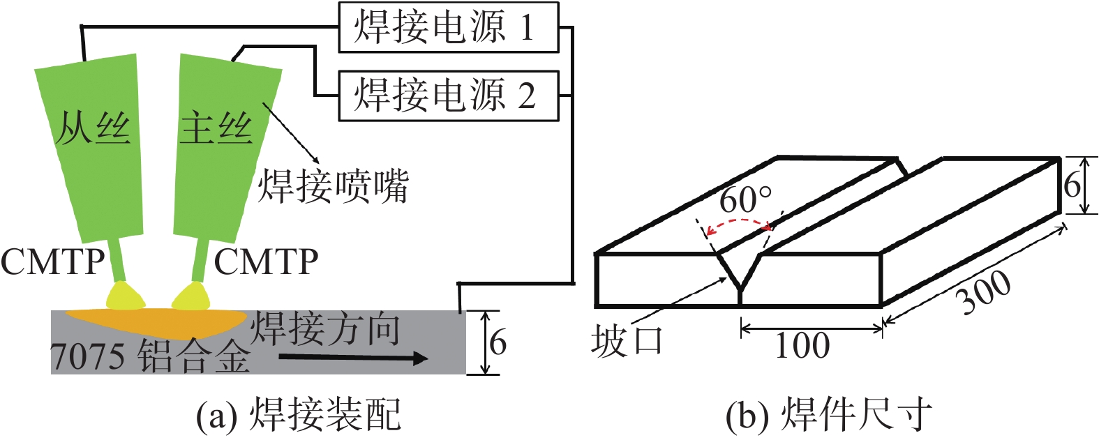
焊接采用Fonius TPS5000CMT双丝焊机. 母材为T6热处理的7075铝合金板,尺寸为300 mm × 100 mm × 6 mm,开有60º坡口. 焊丝为ϕ1.2 mm的ER5356焊丝. 母材和ER5356焊丝的化学成分和力学性能分别见表1和表2. 焊前对母材表面打磨以去除表面氧化膜,并采用丙酮清理表面油污.
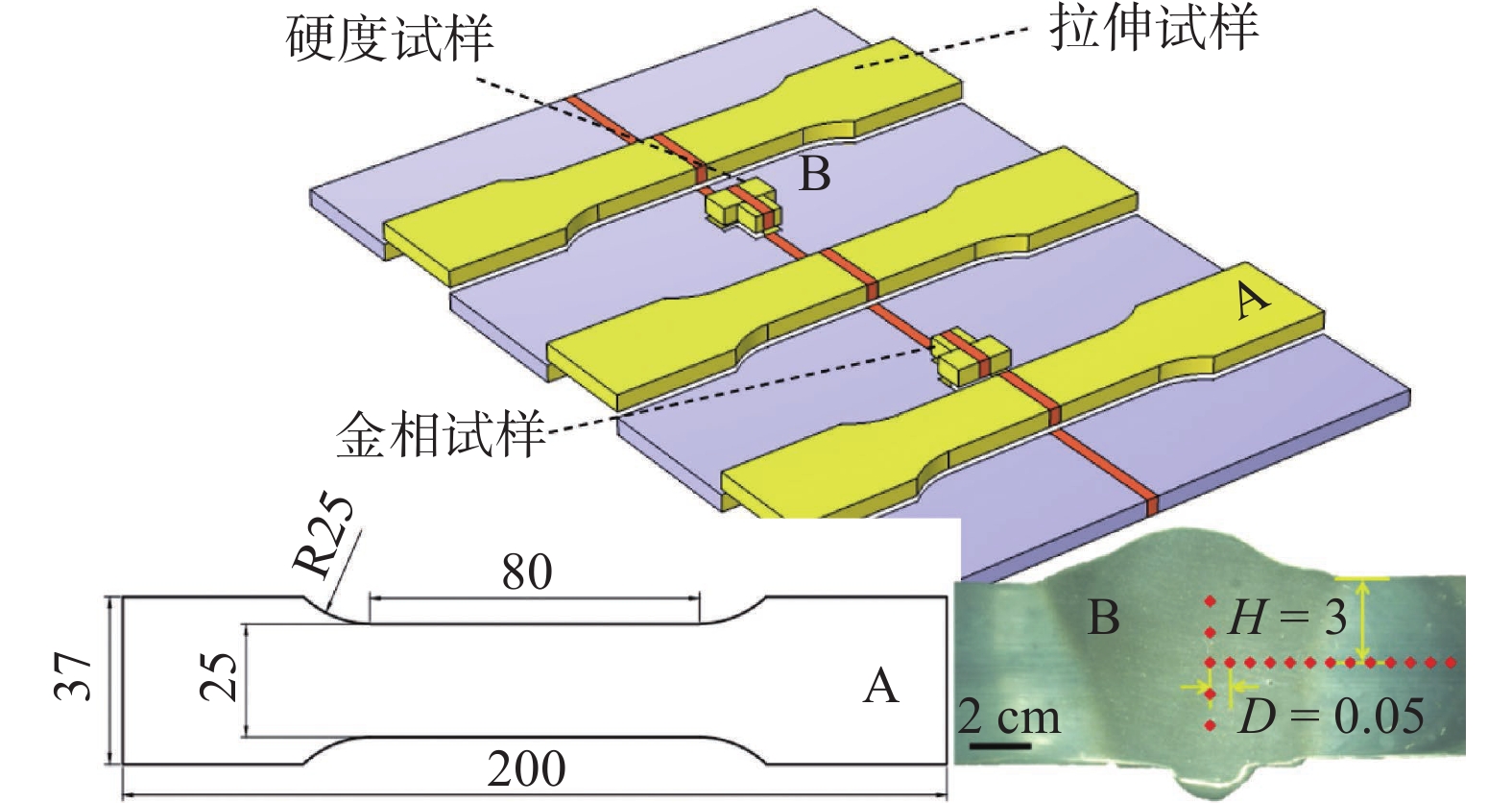
表 1 母材和焊丝的化学成分(质量分数,%)Table 1. Chemical compositions of base metal and welding wire材料 Si Fe Mn Zn Mg Cu Al 7075-T6 0.13 0.24 0.20 6.03 2.22 1.42 余量 ER5356 0.05 0.30 0.16 — 5.050 0.01 余量 表 2 母材和焊丝的力学性能Table 2. Mechanical properties of base metal and welding wire材料 抗拉强度Rm/MPa 屈服强度ReL/MPa 断后伸长率A(%) 7075-T6 548 476 12 ER5356 278 165 21 进行平板对接焊接试验时无预留间隙. 主、从丝夹角为18°,间距为9 mm,电弧挺度为1. 为促进熔深增大并降低热输入,主丝和从丝均采用CMTP电弧,焊接装配及焊件尺寸如图1所示. 焊接速度设置为0.8 mm/min,保护气体为99.99%的氩气,气流量为20 L/min.
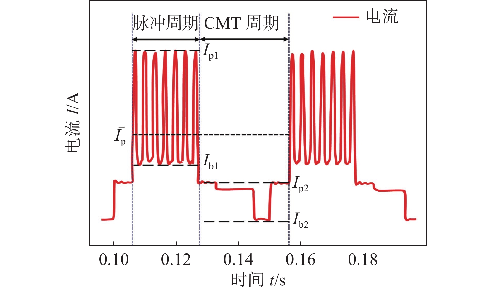
CMTP电流的实测波形如图2所示. 电流由脉冲峰值电流
$ {I}_{\mathrm{p}1} $ 、脉冲基值电流$ {I}_{\mathrm{b}1} $ ,CMT阶段的峰值电流$ {I}_{\mathrm{p}2} $ 和CMT阶段的基值电流$ {I}_{\mathrm{b}2} $ 组成,通过调节主、从丝的峰值脉冲电流改变焊接平均电流$ \overline{{I}_{\mathrm{p}}} $ ;平均电压$ \overline{U} $ 则随峰值电流变化进行调整直至形成稳定电弧. 具体工艺参数见表3. 其中$ {I}_{\mathrm{b}1} $ 、$ {I}_{\mathrm{p}2} $ 和$ {I}_{\mathrm{b}2} $ 为预设不变参数. 为方便描述电流参数,后文中如无特殊说明则电流大小均指实测平均电流大小. CMTP电流的高频脉冲群和短路阶段的基值电流交替变化所形成的电弧压力差促进了熔池搅拌,目前普遍认为,增加脉冲峰值和基值电流的差值($ \Delta I={I}_{\mathrm{p}1}-{I}_{\mathrm{b}1} $ )利于降低焊缝区偏析,然而过大的差值又会导致电弧不稳和熔滴飞溅. 因此,在开展7075-T6铝合金DW-CMTP焊前,需要分别对主、从丝电流大小进行调节,在确保母材熔透和电弧稳定等情况下确定合适的电流区间,再在此基础上通过分别改变主、从丝电流大小进行试验,研究其对焊接效果、接头组织和力学性能的影响.焊接接头力学性能检测取样方法如图3所示. 金相试样经过研磨和抛光后采用凯勒试剂[ϕ(HF)∶ϕ(HCl)∶ϕ(HNO3)∶ϕ(H2O) = 1∶1.5∶2.5∶95]进行腐蚀;采用游标卡尺测量焊缝横截面尺寸,包括焊缝的余高h、熔宽B和焊根宽度d;采用维氏显微硬度计沿焊缝中心向母材水平方向每隔0.05 mm测量一次硬度,并在焊缝中心处沿厚度方向取5个点测量焊缝中心硬度并取其平均值,硬度测量位置如图3中“B”所示;采用万能拉伸机测试接头抗拉强度;采用X射线衍射仪(XRD)和透射电镜(TEM)分析焊缝物相;采用电子背散射衍射(EBSD)分析焊缝组织和晶粒大小;采用金相显微镜和扫描电子显微镜(SEM)观察接头组织、拉伸断裂位置及断口形貌.
表 3 焊接工艺参数Table 3. Welding process parameters组别 主丝
($ {I}_{\mathrm{b}1} $ = 160 A, $ {I}_{\mathrm{p}2} $ = 130 A, $ {I}_{\mathrm{b}2} $ = 50 A)从丝
($ {I^{\prime}}_{\mathrm{b}1} $ = 50 A, $ {I^{\prime}}_{\mathrm{p}2} $ = 45 A, $ {I^{\prime}}_{\mathrm{b}2} $=30 A)$ {I}_{\mathrm{p}1} $/A $\overline{ {I}_{\mathrm{p} } }$/A $\overline{U}$/V $ {I^{\prime}}_{\mathrm{p}1} $/A $\overline{I^{\prime} }_{\mathrm{p} }$/A $\overline{U^{\prime} }$/V B1 330 230 21.4 91 54 2.4 B2 330 230 21.4 133 74 3.7 B3 330 230 21.4 175 94 5.3 B0 330 230 21.4 218 114 7.0 B4 330 230 21.4 260 134 7.0 B5 245 190 20.2 218 114 7.0 B6 287 210 20.9 218 114 7.0 B7 372 250 22.0 218 114 7.0 B8 415 270 24.5 218 114 10.4 2. 结果和讨论
2.1 焊缝形貌
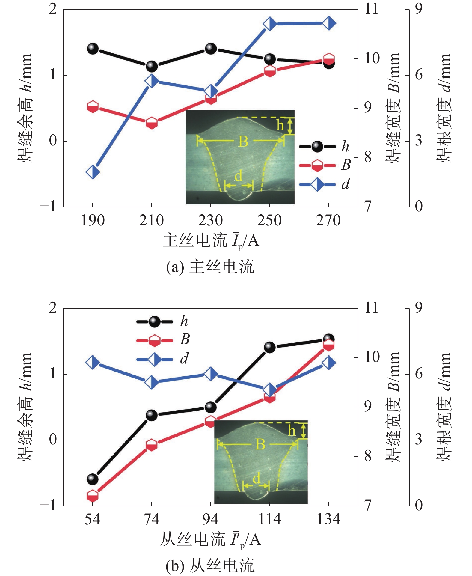
图4显示了DW-CMTP焊接7075-T6铝合金时,主、从丝电流参数变化对焊缝形貌的影响. 熔宽和焊根宽度的尺寸受主丝电流影响较大,表现为随主丝电流的增加而明显增加;而主丝电流的变化对余高的影响却较小;余高和熔宽都随着从丝电流的增加呈现明显上升趋势,而从丝电流大小对焊根宽度的影响较小. 在DW-CMTP焊中,主丝因提供了更多的热输入,对促进熔深有明显作用;而从丝的作用主要是促进熔池流动和增加熔覆率,因而对余高和熔宽的增大有明显作用.
![]() 图 4 焊缝余高、熔宽及焊根宽度随主丝电流和从丝电流变化曲线Figure 4. Dependences of weld reinforcement, weld width and weld root width on leading and trailing wire current. (a) leading wire current; (b) trailing wire current
图 4 焊缝余高、熔宽及焊根宽度随主丝电流和从丝电流变化曲线Figure 4. Dependences of weld reinforcement, weld width and weld root width on leading and trailing wire current. (a) leading wire current; (b) trailing wire current2.2 显微组织
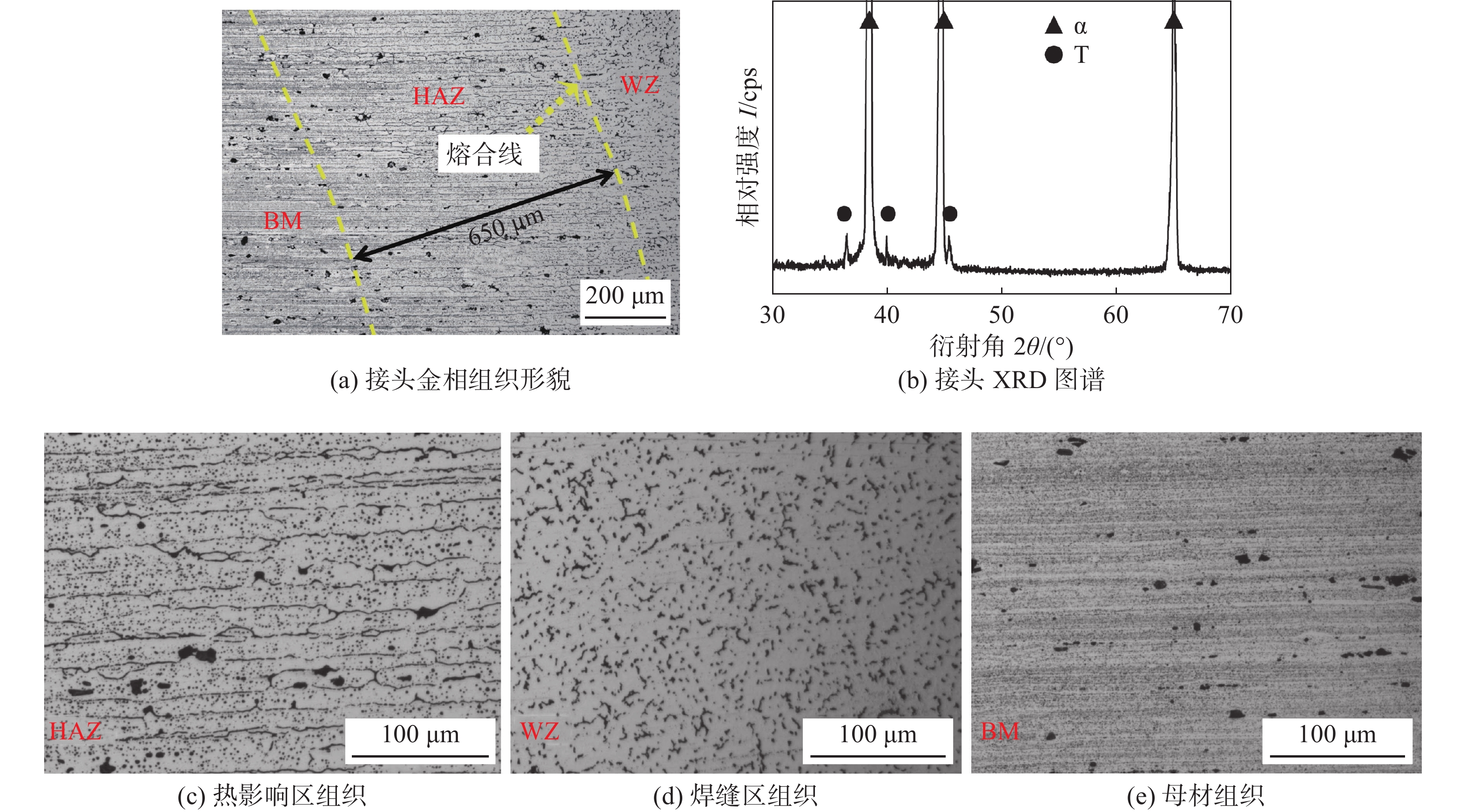
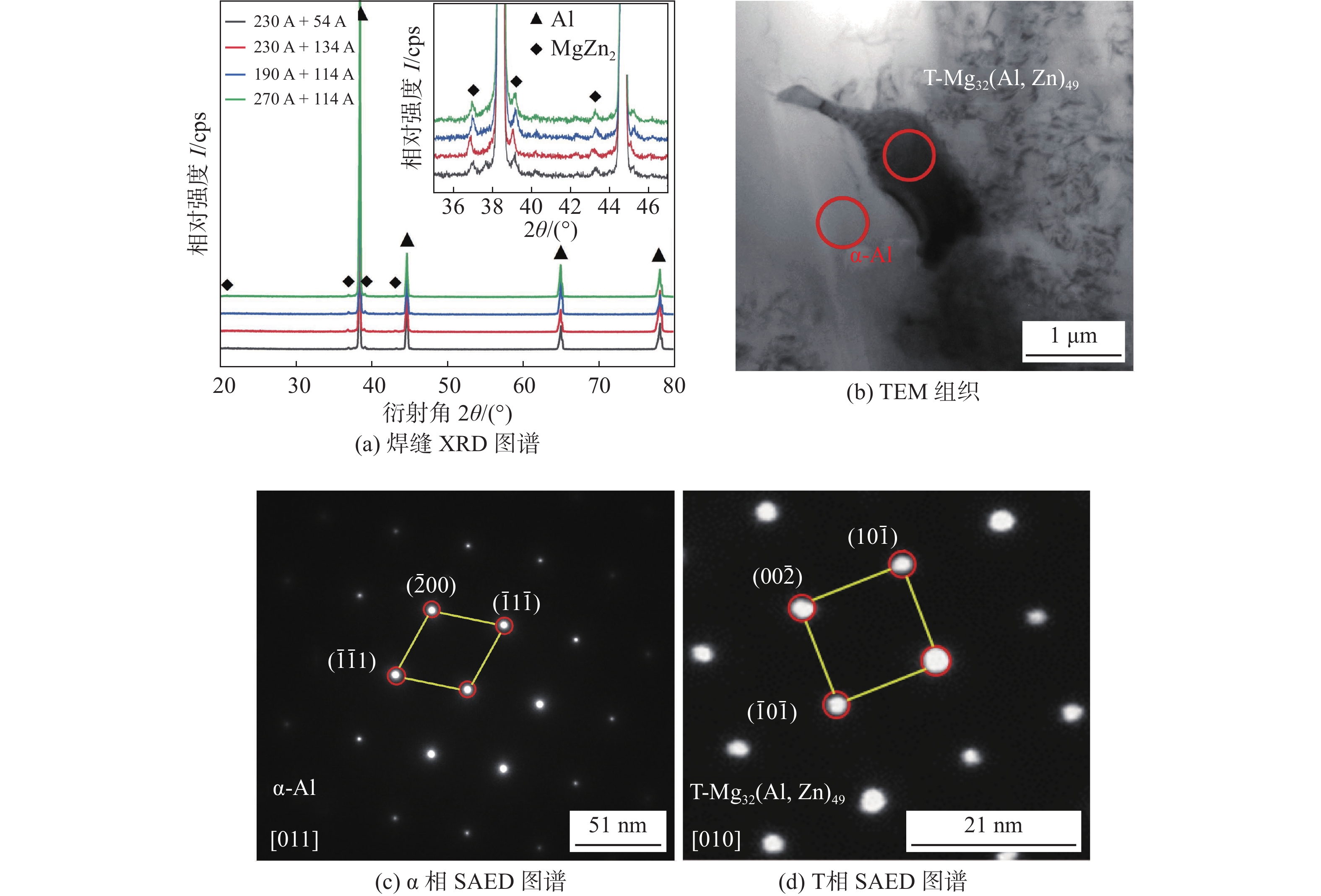
图5为主、从丝电流分别为230 A和114 A时DW-CMTP焊接接头组织形貌及母材XRD图谱. 整个焊接接头从焊缝中心往母材侧可分为3个区域,分别为焊缝区(WZ)、热影响区(HAZ)和母材(BM). 母材为轧制态的7075-T6铝合金组织,以α-Al晶粒为主,伴有弥散分布的η-MgZn2相;HAZ在焊接时处于过热状态,η相发生溶解并伴随着α晶粒长大,冷却过程中因溶解度下降,η相再次析出,HAZ的宽度为600 ~ 900 μm;WZ主要为焊丝及部分母材熔化后形成的铸态枝晶组织. 结合图6的XRD和TEM分析可知,WZ组织主要由α相和T-Mg32(Al, Zn)49相构成. 这是因为焊缝中心较高的Mg/Zn比抑制了η相析出,促进了T相生成.
![]() 图 5 DW-CMTP焊接接头组织形貌(
图 5 DW-CMTP焊接接头组织形貌($ \overline{{I}_{\mathrm{p}}} $ = 230 A 和$ \overline{I\mathrm{^{\prime}}}_{\mathrm{p}} $ = 114 A)及接头XRD图谱.Figure 5. Microstructure of DW-CMTP welded joint ($ \overline{I}_{\mathrm{p}} $ = 230A and$\overline{I\mathrm{^{\prime}}}_{\mathrm{p}}$ = 114 A) and XRD pattern of joint. (a) metallographic morphology of joint; (b) XRD pattern of joint; (c) HAZ microstructure; (d) WZ microstructure; (e) BM microstructure![]() 图 6 不同工艺下焊缝中心处的XRD图谱和主、从丝电流分别为230 A和134 A时焊缝中心组织形貌Figure 6. XRD patterns of the weld center of different welding parameters and TEM image of the weld center responding to 230 A leading wire current and 114 A trailing wire current. (a) XRD pattern of weld center; (b) TEM image; (c) SAED pattern of α phase; (d) SAED pattern of T phase
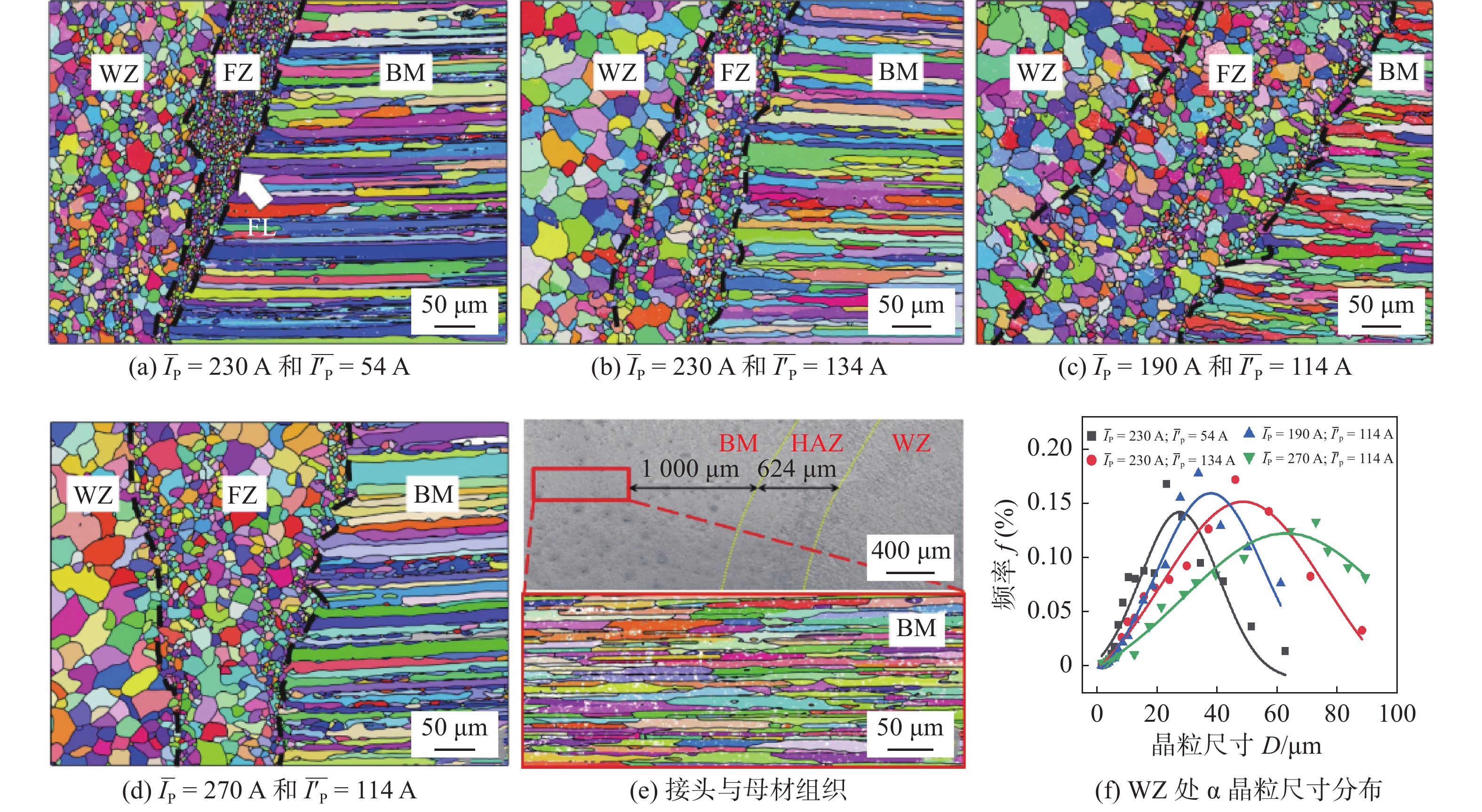
图 6 不同工艺下焊缝中心处的XRD图谱和主、从丝电流分别为230 A和134 A时焊缝中心组织形貌Figure 6. XRD patterns of the weld center of different welding parameters and TEM image of the weld center responding to 230 A leading wire current and 114 A trailing wire current. (a) XRD pattern of weld center; (b) TEM image; (c) SAED pattern of α phase; (d) SAED pattern of T phase为研究电流对焊缝的晶粒大小和晶界取向的影响,文中选取主丝电流为230 A和从丝电流分别为54 A、134 A(增幅为80 A)的B1、B4试样,以及从丝电流为114 A和主丝电流分别为190 A、270 A(增幅为80 A)的B5、B8试样进行EBSD分析,如图7所示. HAZ保留轧制纤维组织特征,与母材组织较为相似,只是晶粒发生了粗化;WZ为较大尺寸的等轴晶组织;WZ与HAZ相邻部位即熔合区(FZ),具有较复杂的微观结构,FZ与母材间形成了不平整的分界面,即熔合线(FL),FZ组织以相对较小的等轴晶组织为主并混有相对较粗的晶粒. 当主丝电流维持230 A恒定,从丝电流由54 A增加至134 A时,WZ中心晶粒尺寸显著增大,FZ附近的细晶区宽度由原本约60 μm增加至约100 μm,这是因为从丝电流的增加促进了熔池的搅拌效果,结晶过程形成的柱状晶被打破,形成细小的晶粒,促进了非均质形核过程的结构起伏条件,使得FZ处的细晶区域宽度增加. 当从丝电流保持114 A恒定,主丝电流从190 A增大至270 A时,WZ中心晶粒发生更明显粗化,细晶区FZ宽度由约240 μm减少至约180 μm,这是因为主丝电流增大,增加了热输入,焊缝熔池在随后冷却过程中冷却速率降低,形核率下降,晶粒尺寸增大,细晶数量减少,从而细晶区宽度降低. 通过对焊缝中心的晶粒取向进行分析,DW-CMTP焊WZ中心处组织基本没有明显晶粒取向,具有各向同性,因此该处在不同方向上表现出相似的力学性能,这与DW-CMTP具有较好的熔池搅拌效果和较低的热输入有关. 当主丝电流较高时,受WZ中心到母材的温度梯度增大的影响,WZ中心的各相同性有轻微减弱.
![]() 图 7 不同主、从丝电流下对应的接头和母材组织的EBSD图以及焊缝中心α晶粒尺寸分布图Figure 7. EBSD graphs of the joints and BM under different leading and trailing current parameters and α grain size distribution of weld center. (a)
图 7 不同主、从丝电流下对应的接头和母材组织的EBSD图以及焊缝中心α晶粒尺寸分布图Figure 7. EBSD graphs of the joints and BM under different leading and trailing current parameters and α grain size distribution of weld center. (a)$ \overline{{I}_{\mathrm{p}}} $ = 230 A and$\overline{I\mathrm{^{\prime}}}_{\mathrm{p}}$ = 54 A; (b)$ \overline{{I}_{\mathrm{p}}} $ = 230 A and$\overline{I\mathrm{^{\prime}}}_{\mathrm{p}}$ = 134 A; (c)$ \overline{{I}_{\mathrm{p}}} $ = 190 A and$\overline{I\mathrm{^{\prime}}}_{\mathrm{p}}$ = 114 A; (d)$ \overline{{I}_{\mathrm{p}}} $ = 270 A and$\overline{I\mathrm{^{\prime}}}_{\mathrm{p}}$ = 114 A; (e) microstructure of joint and BM; (f) α grain size distribution of weld center在传统熔化焊过程中,熔池与母材的固液界面前沿出现成分过冷且未熔母材晶粒表面提供了非均匀形核和散热条件,以致在较小过冷度下便能形核,通常凝固形成的晶粒沿母材表面向焊缝中心方向生长,最终发展成柱状晶组织[14-15],越接近熔池中心,温度梯度越小,因而柱状晶生长减缓,在熔池心部呈现各个方向均匀生长而形成等轴晶[16]. 与传统熔化焊不同的是,DW-CMTP焊缝组织均为等轴晶组织,固液界面并没有发现明显的柱状晶存在. 这一方面是因为高频双丝脉冲电流对熔池形成的搅拌作用破坏了柱状晶的形成和生长,并为结晶提供了驱动力和更多非均质形核核心;另一方面因冷焊丝伸入熔池吸收了大量熔池热,使得散热失去方向性,晶粒生长取向减弱;此外冷焊丝带走的热量也使得熔体保持过冷,从而加快了结晶速度,对形核有促进作用,这也在一定程度上抑制了柱状晶形成,并细化了WZ晶粒,该现象在Chen[17]的研究中也被提及.
2.3 力学性能
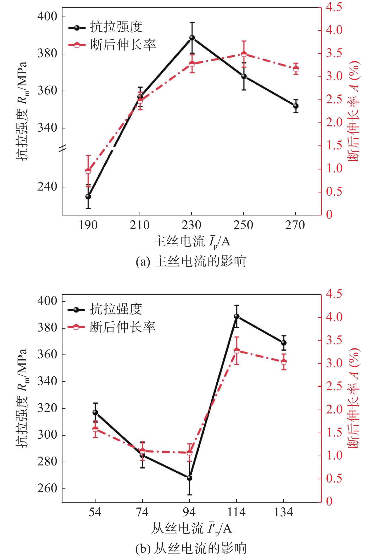
图8显示了主、从丝电流大小对接头抗拉强度和断后伸长率的影响. 当从丝电流恒定为114 A时,接头抗拉强度随主丝电流在190 ~ 270 A范围内增加呈现先增加后降低的趋势;断后伸长率则随主丝电流增加而增加,且主丝电流增大至230 A以后,断后伸长率趋于稳定. 在主丝电流恒定为230 A的条件下,当从丝电流小于94 A时,接头抗拉强度随从丝电流增加呈现逐渐降低的趋势,当从丝电流增至114 A时,接头抗拉强度和断后伸长率急剧上升,而进一步增加从丝电流则使强度和塑性又略有下降. 当主、从丝电流分别为230 A和114 A时,焊接接头获得了最大抗拉强度,为389 MPa,达到了母材抗拉强度的70.8%,此时断后伸长率为3.3%,仅比文中研究的工艺参数范围内获得的最大断后伸长率低0.2%,总体较低的伸长率与熔化焊中不可避免地存在气孔有关.
![]() 图 8 主丝电流(
图 8 主丝电流($\overline{I\mathrm{^{\prime}}}_{\mathrm{p}}$ = 114 A)和从丝电流($ \overline{{I}_{\mathrm{p}}} $ = 230 A)变化对接头抗拉性能的影响Figure 8. Effects of leading wire current ($\overline{I\mathrm{^{\prime}}}_{\mathrm{p}}$ = 114 A) and trailing wire current ($ \overline{{I}_{\mathrm{p}}} $ = 230 A) on joint tensile strength. (a) effect of leading wire current; (b) effect of trailing wire current由于主丝电流的增加,熔池的峰值温度上升,更多母材熔化进入熔池,提高了WZ中Zn元素含量,且降低了WZ中气孔数量,因而接头抗拉强度和断后伸长率也相应上升. 然而,过大的主丝电流则会加重WZ中Zn元素的烧损并导致WZ晶粒粗化,以致接头强度又有所下降而断后伸长率基本不变. 通过观察焊接过程中的电弧,发现当从丝电流明显小于94 A时,从丝电弧的熔滴过渡不稳定,不仅没有起到从丝对熔池的搅拌作用,反而引起熔池飞溅,熔池热量分布严重不均匀,导致WZ部分区域易产生气孔及偏析,降低了接头力学性能;当从丝电流增加至114 A及以上时,电弧稳定性显著提高,从丝电弧不易受主丝电弧的干扰,焊缝力学性能也相应提高,但是过大的从丝电流使得热输入过大,这样反而会失去了利用从丝同时降低WZ温度梯度和熔池温度的效果,引起WZ组织粗化并加重晶间偏析,造成接头强度降低甚至伸长率也略有下降.
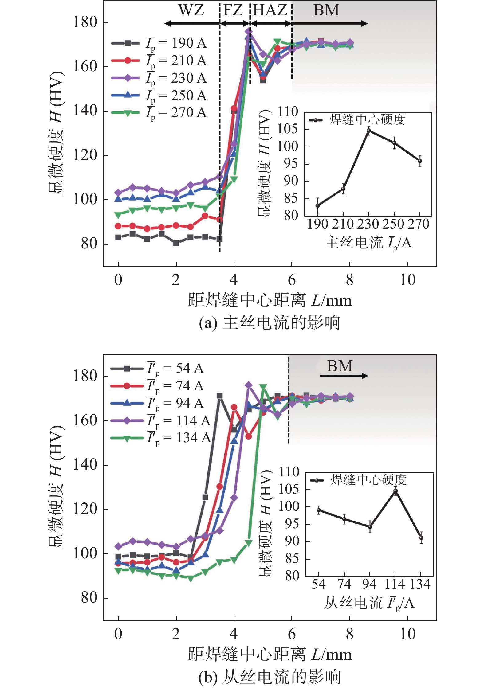
沿焊缝向母材方向的接头硬度分布和焊缝中心平均硬度如图9所示. 在文中研究的所有焊接工艺参数下,WZ的硬度均明显低于HAZ和母材,且在各个不同电流参数下,WZ硬度基本保持稳定. 当从丝电流为114 A和主丝电流在190 ~ 270 A范围内变化时,WZ的宽度基本不变,但WZ中心硬度有明显变化,WZ中心平均硬度最大差值约为HV25;随主丝电流增加,WZ中心平均硬度先增加后减小,230 A时WZ中心的硬度最高. 而保持主丝电流230 A不变,随从丝电流在54 ~ 134 A范围内增大时,WZ宽度逐渐增大,WZ中心硬度也发生了一定程度变化,呈现出先降低后增加再降低的趋势,平均硬度最大差值约为HV15. 当主、从丝电流分别为230 A和114 A时,WZ中心硬度达到最大值(HV104.7). 接头硬度最大值出现在FZ,达到了HV175,硬度增加与该区域形成的细晶组织有关. HAZ的硬度相比于母材有所降低,是此处受热作用晶粒和析出相发生粗化所致,但由于DW-CMTP对热输入的有效控制,其粗化程度并不十分明显,HAZ的硬度仅小幅度下降. 对比图8和图9,WZ处的硬度随主、从丝电流变化趋势与接头抗拉强度的变化趋势基本一致.
![]() 图 9 主丝电流(
图 9 主丝电流($\overline{I\mathrm{^{\prime}}}_{\mathrm{p}}$ = 114 A)和从丝电流($ \overline{{I}_{\mathrm{p}}} $ = 230 A)变化对接头硬度的影响Figure 9. Effects of leading wire current ($\overline{I\mathrm{^{\prime}}}_{\mathrm{p}}$ = 114 A) and trailing wire current ($ \overline{{I}_{\mathrm{p}}} $ = 230 A) on joint hardness. (a) effect of leading wire current; (b) effect of trailing wire current2.4 断口特征及分析
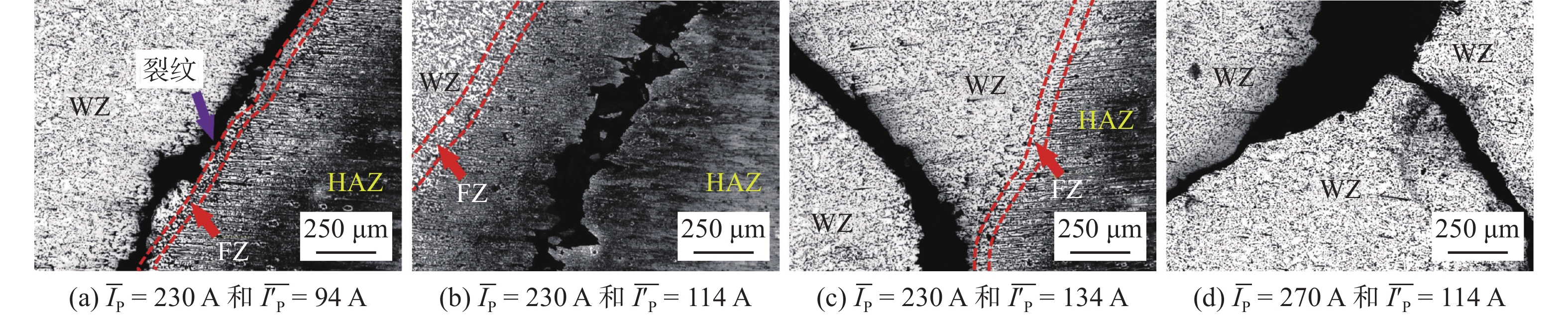
不同工艺参数下获得的接头的拉伸断裂出现在如图10所示的四类位置处. 当从丝电流为114 A且主丝电流小于230 A时,或主丝电流为230 A且从丝电流小于114 A时,断裂发生在如图10a所示的FZ与WZ交界处,略靠近焊缝侧. 主、从丝电流分别为230 A和114 A时,断裂位于图10b所示的HAZ. 当从丝和主丝电流分别高于114 A和230 A时,断裂位置分别如图10c和图10d所示,前者断裂于邻近FZ的WZ,后者则完全断裂于WZ.
![]() 图 10 不同主、从丝电流对应的拉伸断口位置Figure 10. Tensile fracture positions corresponding to different leading and trailing wire currents. (a)
图 10 不同主、从丝电流对应的拉伸断口位置Figure 10. Tensile fracture positions corresponding to different leading and trailing wire currents. (a)$ \overline{{I}_{\mathrm{p}}} $ = 230 A and$\overline{I\mathrm{^{\prime}}}_{\mathrm{p}}$ = 94 A; (b)$ \overline{{I}_{\mathrm{p}}} $ = 230 A and$\overline{I\mathrm{^{\prime}}}_{\mathrm{p}}$ = 114 A; (c)$ \overline{{I}_{\mathrm{p}}} $ = 230 A and$\overline{I\mathrm{^{\prime}}}_{\mathrm{p}}$ =134 A; (d)$ \overline{{I}_{\mathrm{p}}} $ = 270 A and$\overline{I\mathrm{^{\prime}}}_{\mathrm{p}}$ = 114 A为进一步分析产生上述四种不同的断裂位置的原因,对不同焊接工艺参数下的拉伸断口进行观察,如图11所示. 在拉伸断面上可以观察到气孔存在,气孔会减少接头有效承载面积,导致应力集中,降低接头塑性性能,因而试样的断后伸长率总体较低,当焊缝中气孔率降低时,焊缝塑性承载能力增加,塑性相对提高,然而过大的热输入使得焊缝晶粒组织粗大,强度和塑性有所降低. 图11a ~ 11c显示了当主丝电流为230 A,从丝电流在54 ~ 134 A范围内变化时,随从丝电流增大,断面单位面积上的气孔数量虽有明显降低,然而韧窝也变得更浅、更小,这意味着接头塑性有所降低,这与图8b的结果相一致. 图11d ~ 11f显示了当从丝电流为114 A,主丝电流在190 ~ 270 A范围内变化时,断面韧窝形貌变化较小,同时单位面积上气孔数量随主丝电流增加而降低,使得接头抗拉强度和断后伸长率相应增加,但是过高的主丝电流又增加了热输入,使得WZ组织粗化,又会降低接头抗拉强度,甚至断后伸长率也有所下降. 图11g为主、从丝电流分别为230 A和114 A时的断口形貌,不同于其它工艺参数下的断口形貌,该参数下的断口形貌出现了较多的解理台阶,同时韧窝数量明显减少,以脆性主导的断裂为主;由于WZ的气孔数量减少和较细小的晶粒组织增强了WZ的强度和塑性,而HAZ因热输入的增加使得强度和塑性降低,以致断裂位置出现在HAZ处.
![]() 图 11 焊接接头试样拉伸断口形貌及气孔率Figure 11. Tensile fracture morphology of welded joint specimens. (a) B1; (b) B3; (c) B4; (d) B5; (e) B6; (f) B8; (g) B0
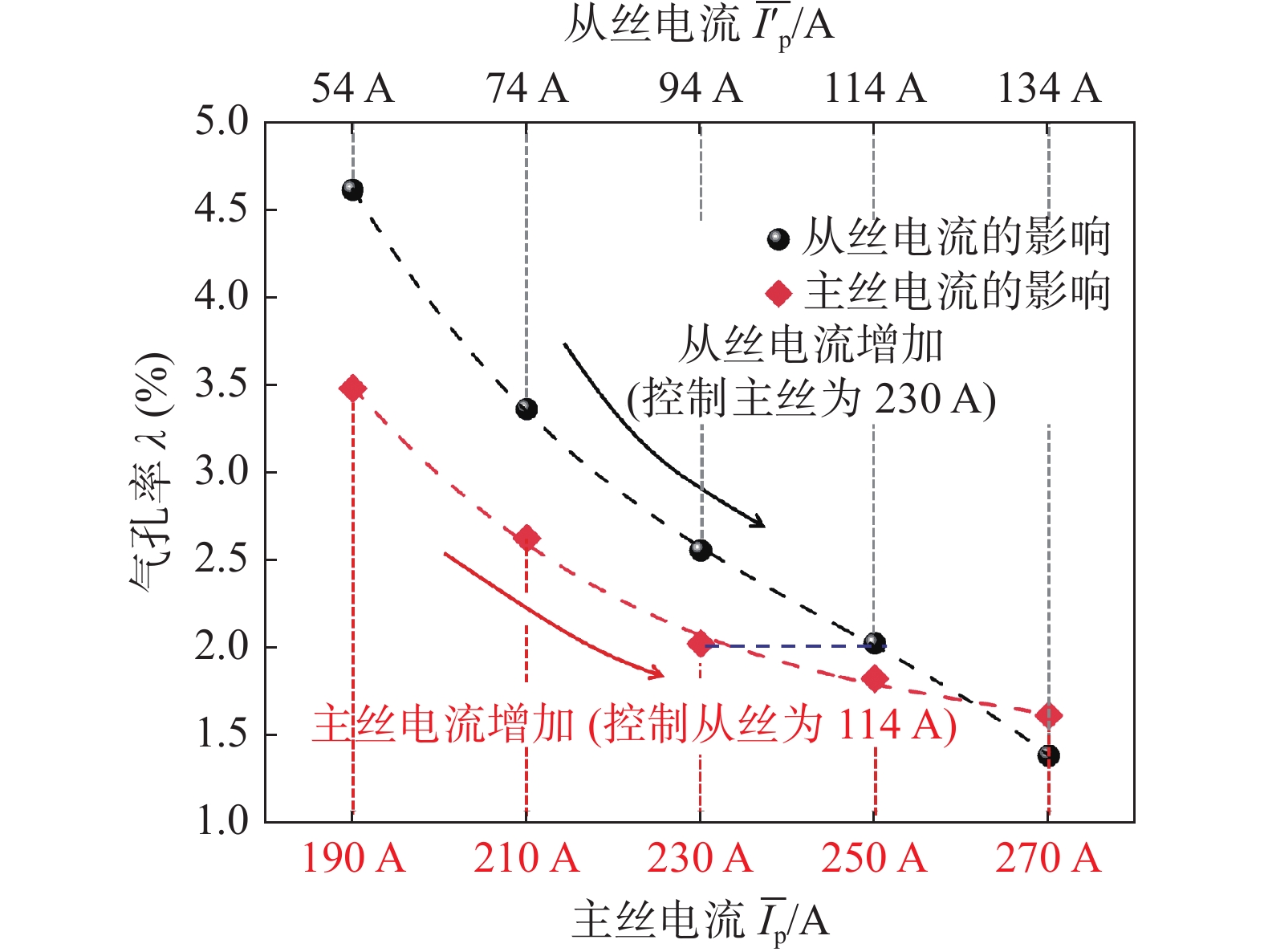
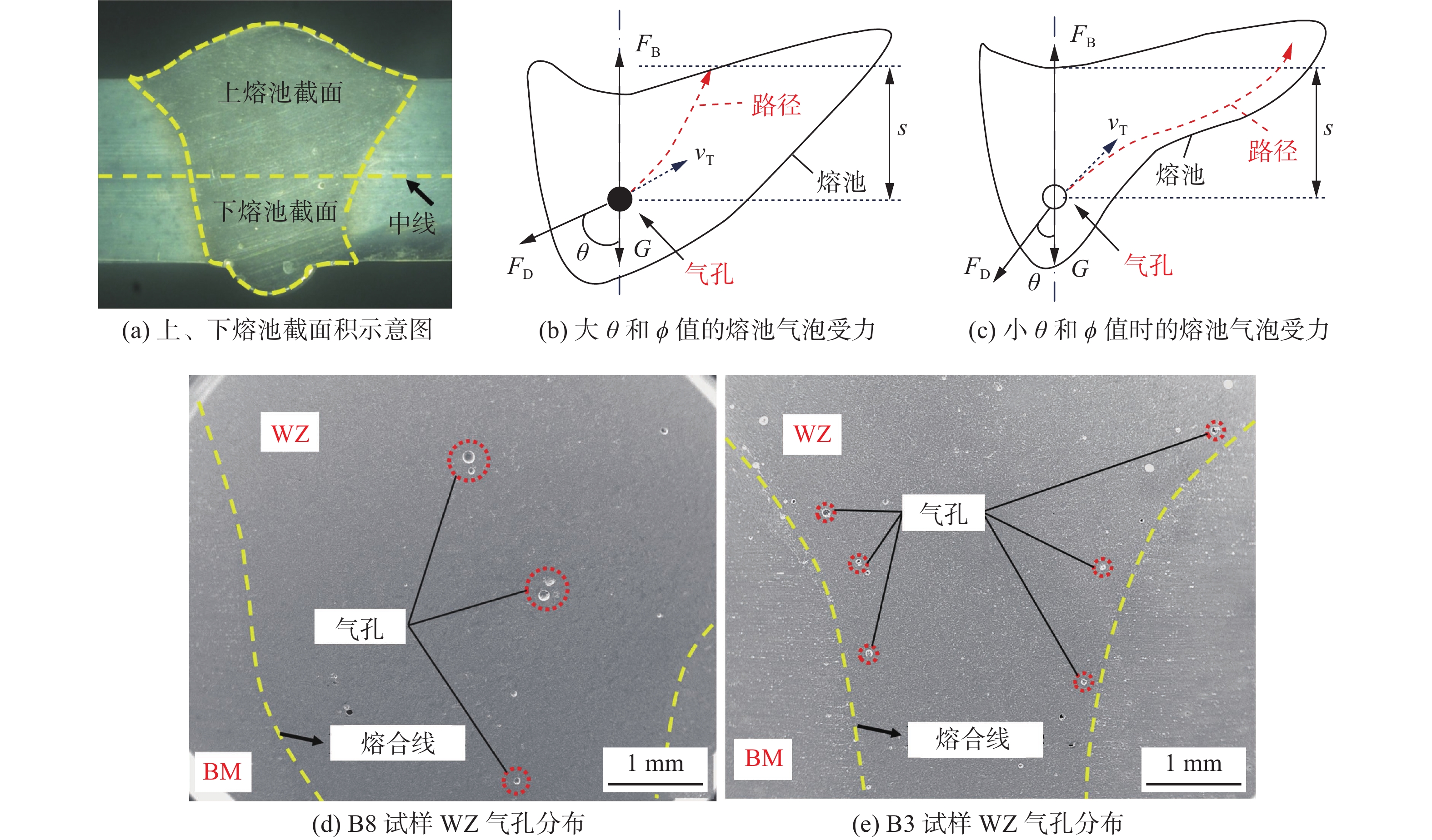
图 11 焊接接头试样拉伸断口形貌及气孔率Figure 11. Tensile fracture morphology of welded joint specimens. (a) B1; (b) B3; (c) B4; (d) B5; (e) B6; (f) B8; (g) B0图12表明在文中研究的工艺参数下,随着主丝和从丝电流的增加,焊缝中的气孔率都呈现下降趋势,然而增加从丝电流对降低气孔率的效果更加显著,推测二者降低气孔率的机制可能并不相同. 从丝电流的增加主要是通过增强熔池流动促进焊缝中气体逸出. 主丝电流增加则倾向于提高熔池温度和增大电弧压力. Katayama等人[18]认为大的电弧压力会加大熔池表面下凹,缩短了气泡上浮到熔池表面的路径,加速了气泡的逸出. 然而DW-CMTP焊具有较大的熔覆率,熔池凹陷并不明显,基于Zhang等人[19]的研究,可推断主丝电流增加提高了下熔池和上熔池体积之比(ϕ),使得气泡上浮速度增加,气孔率降低,如图12a所示,在单位焊缝长度上ϕ可表示为:
$$ \phi =\frac{{S}_{\mathrm{l}\mathrm{o}\mathrm{w}\mathrm{e}\mathrm{r}}}{{S}_{\mathrm{u}\mathrm{p}\mathrm{p}\mathrm{e}\mathrm{r}}} $$ (1) 式中:
$ {S}_{\mathrm{l}\mathrm{o}\mathrm{w}\mathrm{e}\mathrm{r}} $ 和$ {S}_{\mathrm{u}\mathrm{p}\mathrm{p}\mathrm{e}\mathrm{r}} $ 分别为下熔池和上熔池的截面积.气泡在熔池主要受自身重力(G)、浮力(FB)和黏滞阻力(FD)的作用,如图13所示. 因而气泡从底部逸出的加速度
$ a $ 可表示为:![]() 图 13 熔池中气泡受力情况和DW-CMTP焊接接头气孔分布Figure 13. Force condition of bubble in weld pool and pore distribution of in DW-CMTP welded joint. (a) schematics of the cross-sectional area of upper and lower weld pool; (b) force condition of bubble under bigger θ and ϕ; (c) force condition of bubble under smaller θ and ϕ; (d) pore distribution of WZ in sample B8; (e) pore distribution of WZ in sample B3
图 13 熔池中气泡受力情况和DW-CMTP焊接接头气孔分布Figure 13. Force condition of bubble in weld pool and pore distribution of in DW-CMTP welded joint. (a) schematics of the cross-sectional area of upper and lower weld pool; (b) force condition of bubble under bigger θ and ϕ; (c) force condition of bubble under smaller θ and ϕ; (d) pore distribution of WZ in sample B8; (e) pore distribution of WZ in sample B3$$ a=\frac{{F}_{\rm{B}}-G-{F}_{\rm{D}}\rm{cos}\theta }{\dfrac{1}{6}{\text{π}}{D}^{3}{\rho }_{\rm{g}}}=\frac{{\rho }_{\rm{m}}-{\rho }_{\rm{g}}}{{\rho }_{\rm{g}}}g-\frac{18\mu {v}_{\rm{T}}\rm{cos}\theta }{{D}^{2}{\rho }_{\rm{g}}} $$ (2) 式中,
$ \mu $ ;D;$ {v}_{\mathrm{T}} $ ;$ g $ ;$ {\rho }_{\mathrm{m}} $ 和$ {\rho }_{\mathrm{g}} $ 分别表示熔池黏度系数、气泡直径、熔池流动速度、重力加速度、熔液液体密度和气泡密度;$ \theta $ 为黏滞阻力方向与竖直方向的夹角,与下熔池轮廓有关,随ϕ值的增加而增加.DW-CMTP焊接过程中主丝电流的增加在增大熔深的同时也增大了焊根宽度,增加了下熔池的体积,使得ϕ值增加,这意味着
$ \theta $ 增加,从而加大了气泡上浮的加速度,气泡倾向于沿竖直向上方向逃逸,气泡能沿着更短的路径更快逸出(图12b),最终导致气孔易出现在如图12d所示的焊缝中心位置,因而在较大的主丝电流下断裂位置易发生于图10d所示的WZ中心位置;反之,低主丝电流下的因热输入低,下熔池体积减小,因而ϕ值和$ \theta $ 值较小,气泡上浮的加速度也相应较小,气泡逸出路径增加,因而气泡上浮慢且倾向于沿熔合线逸出(图12c),最终导致气孔易出现在如图12e所示的熔合线附近,因而断裂易产生于此处. 上述两种情况主要考虑了气孔诱发断裂. 实际上,虽然电流的增加会降低气孔率,然而过大的电流会导致焊缝区晶粒粗化,适当控制热输入,既有利于降低气孔率,又可以获得细小的晶粒组织,从而提高WZ强度,进而提高接头抗拉强度. 主丝和从丝电流分别为230 A和114 A时(对应B0试样),WZ气孔率相对较低且晶粒细小以致其WZ强度高于HAZ,拉伸时断裂发生于HAZ.3. 结论
(1)双丝脉冲冷金属过渡焊接过程中,主丝电流主要提供热输入,随主丝电流增大,熔深和焊根宽度增加明显;从丝则利于降低熔池热输入,增大从丝电流可促进熔池流动和提高熔覆率.
(2)主、从丝电流增大分别通过增大气泡上浮力和增强熔池流动而促进焊缝中气体逸出,且增大从丝电流对降低焊缝气孔率的效果更明显.
(3)接头抗拉强度受主丝电流变化的影响相对较大,随主丝电流的增加呈先增加后降低趋势,随从丝电流增加则呈先降低后增加趋势. 主、从丝电流分别为230 A和114 A时获得的接头焊缝中气孔率相对较低且晶粒细小而具有最大强度389 MPa,达到了母材的70.8%.
-
![]()
图 4 焊缝余高、熔宽及焊根宽度随主丝电流和从丝电流变化曲线
Figure 4. Dependences of weld reinforcement, weld width and weld root width on leading and trailing wire current. (a) leading wire current; (b) trailing wire current
![]()
图 5 DW-CMTP焊接接头组织形貌(
$ \overline{{I}_{\mathrm{p}}} $ = 230 A 和$ \overline{I\mathrm{^{\prime}}}_{\mathrm{p}} $ = 114 A)及接头XRD图谱.Figure 5. Microstructure of DW-CMTP welded joint (
$ \overline{I}_{\mathrm{p}} $ = 230A and$\overline{I\mathrm{^{\prime}}}_{\mathrm{p}}$ = 114 A) and XRD pattern of joint. (a) metallographic morphology of joint; (b) XRD pattern of joint; (c) HAZ microstructure; (d) WZ microstructure; (e) BM microstructure![]()
图 6 不同工艺下焊缝中心处的XRD图谱和主、从丝电流分别为230 A和134 A时焊缝中心组织形貌
Figure 6. XRD patterns of the weld center of different welding parameters and TEM image of the weld center responding to 230 A leading wire current and 114 A trailing wire current. (a) XRD pattern of weld center; (b) TEM image; (c) SAED pattern of α phase; (d) SAED pattern of T phase
![]()
图 7 不同主、从丝电流下对应的接头和母材组织的EBSD图以及焊缝中心α晶粒尺寸分布图
Figure 7. EBSD graphs of the joints and BM under different leading and trailing current parameters and α grain size distribution of weld center. (a)
$ \overline{{I}_{\mathrm{p}}} $ = 230 A and$\overline{I\mathrm{^{\prime}}}_{\mathrm{p}}$ = 54 A; (b)$ \overline{{I}_{\mathrm{p}}} $ = 230 A and$\overline{I\mathrm{^{\prime}}}_{\mathrm{p}}$ = 134 A; (c)$ \overline{{I}_{\mathrm{p}}} $ = 190 A and$\overline{I\mathrm{^{\prime}}}_{\mathrm{p}}$ = 114 A; (d)$ \overline{{I}_{\mathrm{p}}} $ = 270 A and$\overline{I\mathrm{^{\prime}}}_{\mathrm{p}}$ = 114 A; (e) microstructure of joint and BM; (f) α grain size distribution of weld center![]()
图 8 主丝电流(
$\overline{I\mathrm{^{\prime}}}_{\mathrm{p}}$ = 114 A)和从丝电流($ \overline{{I}_{\mathrm{p}}} $ = 230 A)变化对接头抗拉性能的影响Figure 8. Effects of leading wire current (
$\overline{I\mathrm{^{\prime}}}_{\mathrm{p}}$ = 114 A) and trailing wire current ($ \overline{{I}_{\mathrm{p}}} $ = 230 A) on joint tensile strength. (a) effect of leading wire current; (b) effect of trailing wire current![]()
图 9 主丝电流(
$\overline{I\mathrm{^{\prime}}}_{\mathrm{p}}$ = 114 A)和从丝电流($ \overline{{I}_{\mathrm{p}}} $ = 230 A)变化对接头硬度的影响Figure 9. Effects of leading wire current (
$\overline{I\mathrm{^{\prime}}}_{\mathrm{p}}$ = 114 A) and trailing wire current ($ \overline{{I}_{\mathrm{p}}} $ = 230 A) on joint hardness. (a) effect of leading wire current; (b) effect of trailing wire current![]()
图 10 不同主、从丝电流对应的拉伸断口位置
Figure 10. Tensile fracture positions corresponding to different leading and trailing wire currents. (a)
$ \overline{{I}_{\mathrm{p}}} $ = 230 A and$\overline{I\mathrm{^{\prime}}}_{\mathrm{p}}$ = 94 A; (b)$ \overline{{I}_{\mathrm{p}}} $ = 230 A and$\overline{I\mathrm{^{\prime}}}_{\mathrm{p}}$ = 114 A; (c)$ \overline{{I}_{\mathrm{p}}} $ = 230 A and$\overline{I\mathrm{^{\prime}}}_{\mathrm{p}}$ =134 A; (d)$ \overline{{I}_{\mathrm{p}}} $ = 270 A and$\overline{I\mathrm{^{\prime}}}_{\mathrm{p}}$ = 114 A![]()
图 11 焊接接头试样拉伸断口形貌及气孔率
Figure 11. Tensile fracture morphology of welded joint specimens. (a) B1; (b) B3; (c) B4; (d) B5; (e) B6; (f) B8; (g) B0
![]()
图 13 熔池中气泡受力情况和DW-CMTP焊接接头气孔分布
Figure 13. Force condition of bubble in weld pool and pore distribution of in DW-CMTP welded joint. (a) schematics of the cross-sectional area of upper and lower weld pool; (b) force condition of bubble under bigger θ and ϕ; (c) force condition of bubble under smaller θ and ϕ; (d) pore distribution of WZ in sample B8; (e) pore distribution of WZ in sample B3
表 1 母材和焊丝的化学成分(质量分数,%)
Table 1 Chemical compositions of base metal and welding wire
材料 Si Fe Mn Zn Mg Cu Al 7075-T6 0.13 0.24 0.20 6.03 2.22 1.42 余量 ER5356 0.05 0.30 0.16 — 5.050 0.01 余量  下载: 导出CSV
表 2 母材和焊丝的力学性能
Table 2 Mechanical properties of base metal and welding wire
材料 抗拉强度Rm/MPa 屈服强度ReL/MPa 断后伸长率A(%) 7075-T6 548 476 12 ER5356 278 165 21
下载: 导出CSV
表 3 焊接工艺参数
Table 3 Welding process parameters
组别 主丝
($ {I}_{\mathrm{b}1} $ = 160 A,$ {I}_{\mathrm{p}2} $ = 130 A,$ {I}_{\mathrm{b}2} $ = 50 A)从丝
($ {I^{\prime}}_{\mathrm{b}1} $ = 50 A,$ {I^{\prime}}_{\mathrm{p}2} $ = 45 A,$ {I^{\prime}}_{\mathrm{b}2} $ =30 A)$ {I}_{\mathrm{p}1} $ /A$\overline{ {I}_{\mathrm{p} } }$ /A$\overline{U}$ /V$ {I^{\prime}}_{\mathrm{p}1} $ /A$\overline{I^{\prime} }_{\mathrm{p} }$ /A$\overline{U^{\prime} }$ /VB1 330 230 21.4 91 54 2.4 B2 330 230 21.4 133 74 3.7 B3 330 230 21.4 175 94 5.3 B0 330 230 21.4 218 114 7.0 B4 330 230 21.4 260 134 7.0 B5 245 190 20.2 218 114 7.0 B6 287 210 20.9 218 114 7.0 B7 372 250 22.0 218 114 7.0 B8 415 270 24.5 218 114 10.4
下载: 导出CSV
-
[1] Lee W S, Lin C R. Deformation behavior and microstructural evolution of 7075-T6 aluminum alloy at cryogenic temperatures[J]. Cryogenics, 2016, 79: 26 − 34. doi: 10.1016/j.cryogenics.2016.07.007
[2] Pickin C G, Young K. Evaluation of cold metal transfer (CMT) process for welding aluminium alloy[J]. Science and Technology of Welding and Joining, 2013, 11(5): 583 − 585.
[3] Alatorre N, Ambriz R R, Noureddine B, et al. Tensile properties and fusion zone hardening for GMAW and MIEA welds of a 7075-T651 aluminum alloy[J]. Acta Metallurgica Sinica (English Letters), 2014, 27(4): 694 − 704. doi: 10.1007/s40195-014-0103-x
[4] 刘长军, 刘政军, 阮祥钢, 等. 焊后热处理对AA7075铝合金DP-MIG焊接接头组织及力学性能的影响[J]. 焊接学报, 2016, 37(10): 81 − 84,88. Liu Changjun, Liu Zhengjun, Ruan Xianggang, et al. Effect of post-weld heat treatment on microstructure and mechanical properties of welded joint of 7075 aluminum alloy by double-plused metal inert-gas welding process[J]. Transactions of the China Welding Institution, 2016, 37(10): 81 − 84,88.
[5] Yang K, Wang F, Liu H B, et al. Double-pulse triple-wire MIG welding of 6082-T6 aluminum alloy: process characteristics and joint performances[J]. Metals, 2021, 11(9): 1388. doi: 10.3390/met11091388
[6] Liu A H, Tang X H, Lu F G. Weld pool profile characteristics of Al alloy in double-pulsed GMAW[J]. The International Journal of Advanced Manufacturing Technology, 2013, 68: 2015 − 2023. doi: 10.1007/s00170-013-4808-1
[7] Wu K Y, Liang Z Y, Yin T, et al. Double pulse low-frequency modulation for high-power double-wire pulsed GMAW[J]. Journal of Manufacturing Science and Engineering, 2018, 140(9): 091004. doi: 10.1115/1.4040319
[8] Alatorre N, Ambriz R R, Amrouche A, et al. Fatigue crack growth in Al-Zn-Mg (7075-T651) welds obtained by modified indirect and gas metal arc welding techniques[J]. Journal of Materials Processing Technology, 2017, 248: 207 − 217. doi: 10.1016/j.jmatprotec.2017.05.025
[9] Yang B J, Fu Z H, Li T, et al. Microstructure and fracture toughness properties of CMT repairing welded 7075-T651 MIG welding joint[J]. Materials Research Express, 2019, 6(12): 1265d6.
[10] Selvi S, Vishvaksenan A, Rajasekar E. Cold metal transfer (CMT) technology-an overview[J]. Defence Technology, 2018, 14(1): 28 − 44. doi: 10.1016/j.dt.2017.08.002
[11] Gandhi C, Dixit N, Aranke O, et al. Characterization of AA7075 weldment using CMT process[J]. Materials Today: Proceedings, 2018, 5(11): 24024 − 24032. doi: 10.1016/j.matpr.2018.10.195
[12] Elrefaey A. Effectiveness of cold metal transfer process for welding 7075 aluminium alloys[J]. Science and Technology of Welding and Joining, 2015, 20(4): 280 − 285. doi: 10.1179/1362171815Y.0000000017
[13] Li J J, Shen J Q, Hu S S, et al. Microstructure and mechanical properties of 6061/7N01 CMT + P joints[J]. Journal of Materials Processing Technology, 2019, 264: 134 − 144. doi: 10.1016/j.jmatprotec.2018.09.011
[14] Liang Y, Hu S S, Shen J Q, et al. Geometrical and microstructural characteristics of the TIG-CMT hybrid welding in 6061 aluminum alloy cladding[J]. Journal of Materials Processing Technology, 2017, 239: 18 − 30. doi: 10.1016/j.jmatprotec.2016.08.005
[15] Hu B, Richardson I M. Microstructure and mechanical properties of AA7075(T6) hybrid laser/GMA welds[J]. Materials Science and Engineering:A, 2007, 459(1-2): 94 − 100. doi: 10.1016/j.msea.2006.12.094
[16] Geng S N, Jiang P, Shao X Y, et al. Heat transfer and fluid flow and their effects on the solidification microstructure in full-penetration laser welding of aluminum sheet[J]. Journal of Materials Science & Technology, 2020, 46: 50 − 63.
[17] Chen D, Cai Y H, Luo Y, et al. Analysis on the microstructure regulation based on the pulsed laser oscillating molten pool in Laser-PTA additive manufacturing[J]. Journal of Manufacturing Processes, 2020, 59: 587 − 594. doi: 10.1016/j.jmapro.2020.10.004
[18] Katayama S, Naito Y, Uchiumi S, et al. Physical phenomena and porosity prevention mechanism in laser-arc hybrid welding[J]. Transactions of JWRI, 2006, 35(1): 13 − 18.
[19] Zhang C, Gao M, Wang D Z, et al. Relationship between pool characteristic and weld porosity in laser arc hybrid welding of AA6082 aluminum alloy[J]. Journal of Materials Processing Technology, 2017, 240: 217 − 222. doi: 10.1016/j.jmatprotec.2016.10.001
-
期刊类型引用(3)
1. 方迪生,凡园园,黄瑞生,徐富家,裴亮,李嘉实. 厚板5A06铝合金万瓦级扫描激光立焊组织与性能. 焊接学报. 2024(06): 68-76 .  本站查看
本站查看
2. 邱飒蔚,蒋家传,叶拓,张越,雷贝,王涛. AA7075-T6铝合金电阻点焊工艺参数优化研究. 材料导报. 2024(17): 258-265 . 百度学术
3. 綦秀玲,张勇. 随焊冲击对6061铝合金焊接接头性能影响. 兵器材料科学与工程. 2023(03): 48-53 . 百度学术
其他类型引用(0)


计量
- 文章访问数: 454
- HTML全文浏览量: 71
- PDF下载量: 58
- 被引次数: 3
