
Finite element analysis of solder joint reliability of 3D packaging chip
-
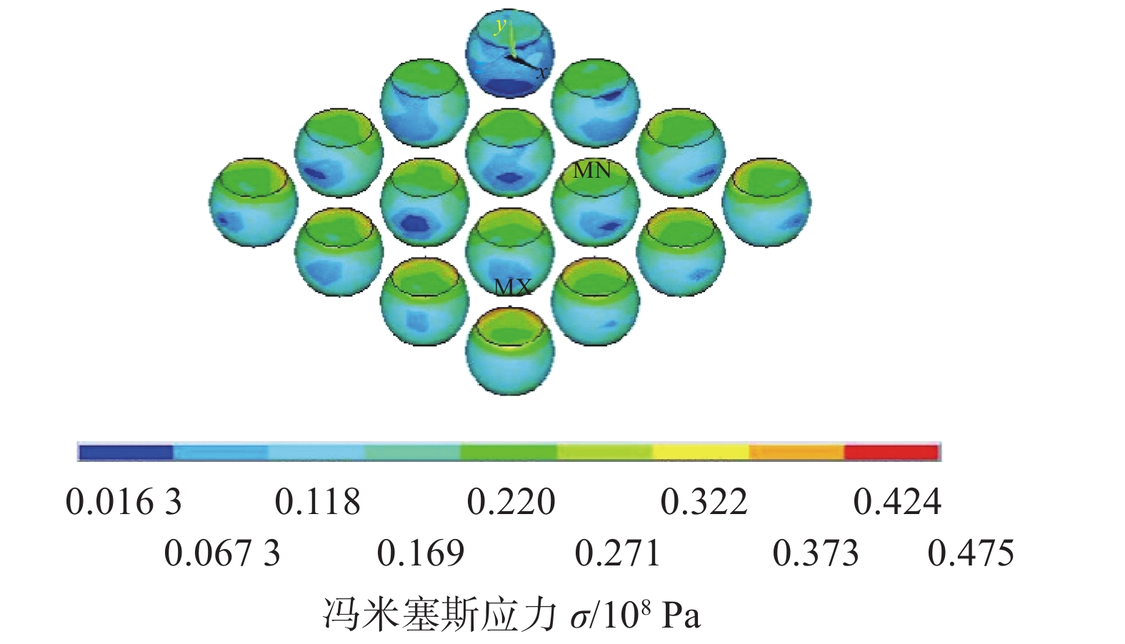
摘要: 选择工业中广泛使用的Sn,Sn3.9Ag0.6Cu钎料作为三维封装芯片键合焊点材料,采用ANSYS有限元软件建立三维封装模型,基于Garofalo-Arrhenius本构方程,进行−55 ~ 125 °C热循环模拟,并通过田口法探讨封装结构和工艺参数对焊点的可靠性影响. 结果表明,Cu柱与焊点接触处是整个结构的薄弱区域,在IMC焊点阵列中最右列第二个焊点处出现最大应力. 通过田口法,结合有限元模拟结果,获得了4个因子对S/N的贡献度由大到小依次为:焊点阵列、焊点高度、芯片厚度、焊点材料. 其中焊点阵列的影响最大,其次是焊点高度、芯片厚度,焊点材料影响最小. 基于优化设计,获得了最优的匹配组合为3 × 3阵列,焊点高度0.02 mm,芯片厚度0.2 mm,焊点材料Cu6Sn5.Abstract: In this paper, Sn and Sn3.9Ag0.6Cu solders, which are widely used in industry, were selected as bonding materials for 3D packaging chips. The 3D packaging model was established using ANSYS finite element software. Based on the Garofalo-Arminius’s constitutive equation, the process of thermal cycle under the temperature condition from −55 ~ 125 °C. In addition, the influence of packaging structure and process parameters on the reliability of solder joint was discussed by Taguchi method. The results show that the contact area between Cu pillar and solder joint is the weak area of the whole structure, and the maximum stress appears at the second solder joint in the rightmost row of the intermetallic compound (IMC) solder joint array. Through the Taguchi method and combined with the finite element simulation results, the contribution of the four factors to S/N was obtained as follows: solder joint array, solder joint height, chip thickness, solder joint material, of which the solder joint array has the largest influence, followed by solder joint height and chip thickness, solder joint material has the least influence. Based on the optimization design, the optimal matching combination was solder joint array 3 × 3, solder joint height 0.02 mm, chip thickness 0.2 mm and solder joint material Cu6Sn5.
-
Keywords:
- 3D packaging /
- reliability of solder joint /
- stress distribution /
- Taguchi method
-
0. 序言
铝合金因其质量轻、比强度高、耐蚀性好等优点被广泛应用于航空航天、汽车制造等重要领域[1-2].其中2219和5A06铝合金是应用广泛的典型代表,2219铝合金比强度高,5A06铝合金耐蚀性好,两者由于性能的差异被用于不同的场合[3-4]. 随着结构服役情况的不断提高,为同时满足结构件高强度及耐蚀性的需求,对异种铝合金焊接接头性能提出了更高要求[5-6].
焊接接头的最终性能取决于焊接工艺参数的选择,选择合适的工艺参数将会极大地提高接头的质量, 因此进行一系列合理的试验来确定最佳的工艺参数至关重要. 然而全面试验方法需要大量的试验次数来确定最佳工艺参数,这很显然需要消耗大量的时间及成本[7]. 相比于全面试验方法,正交试验方法是从全面试验中挑选出部分有代表性的点进行试验,并且能够利用数理统计的方法处理试验结果[8], 因而减少了试验次数,具有较高的效率,得到了国内外研究学者的广泛应用[9-10].
文中采用正交试验方法对2219/5A06异种铝合金脉冲变极性钨极氩弧焊 (variable polarity tungsten inert gas welding, VP-TIG) 进行工艺参数优化,并通过试验分析优化后焊接接头组织与性能的相关性,为异种铝合金接头性能的研究提供试验依据.
1. 试验方法
母材为热处理强化的2219-T87铝合金和加工硬化的5A06-H112铝合金,试板规格为150 mm × 75 mm × 5.5 mm. 为了获得较高强度的焊接接头,采用ER2319铝合金焊丝,焊丝直径1.2 mm, 母材及焊丝化学成分如表1所示,焊接电源为山东奥太WSME-315型逆变式交直流脉冲氩弧焊机.
表 1 母材和ER2319焊丝化学成分Table 1. Chemicial compositions of the base material and the ER2319 welding wire材料 Si Fe Cu Mn Mg Zn Ti Zr Al 其它 2219-T87 0.2 0.3 5.8 ~ 6.8 0.2 ~ 0.4 0.02 0.1 0.02 ~ 0.1 0.10 ~ 0.25 余量 V:0.050 0 ~ 0.150 0 5A06-H112 0.4 0.4 0.1 0.5 ~ 0.8 5.80 ~ 6.80 0.2 0.02 ~ 0.1 - 余量 Be:0.000 1 ~ 0.005 0 ER2319 0.2 0.3 5.8 ~ 6.8 0.2 ~ 0.4 0.20 0.1 0.10 ~ 0.20 0.10 ~ 0.25 余量 V:0.050 0 ~ 0.150 0 焊接过程中,需保持以下工艺参数恒定不变:基值电流Ib = 180 A,占空比δ = 50%,交流频率100 Hz,保护气体为99.99%纯氩气,气体流量15 L/min,钨极到工件的距离为3 mm,V形坡口钝边2 mm,无根部间隙,焊接方向垂直于轧制方向. 为了保证阴极清理的前提下,最大程度地降低钨极的烧损,将脉冲变极性氩弧焊机设置交流偏置Ki = 10%(负半波电流/正半波电流为1.1时,KI = 10%),清理比例Kt = −20%(负半波时间/工作周期为0.3时,Kt = −20%).
按国家标准GB/T 228.1—2010进行拉伸试验,拉伸速率为1 mm/min,通过数字图像相关 (digital image correlation, DIC) 技术测量拉伸过程中实时的应变分布云图,采用ZEISS Sigma 300场发射扫描电镜、Zeiss Smart Zooms 5超景深显微镜、SU-1510扫描电镜观察断口形貌. 按国家标准GB/T 2654—2008进行显微硬度测试,试验加载力为4.9 N,加载时间15 s. 采用传统的三电极Autolab电化学工作站在3.5%NaCl溶液中进行循环电化学极化测试,分析2219侧铝合金和焊缝的点蚀行为.
2. 正交试验
2.1 建立正交模型
正交试验方法按以下步骤进行:① 选因素(脉冲VP-TIG焊工艺参数)、定水平(工艺参数的变化范围); ②选择合适正交表;③ 进行正交试验,记录质量特征值(抗拉强度);④ 采用Minitab软件对试验结果进行数理统计分析;⑤进行最佳参数验证试验.脉冲VP-TIG焊可调工艺参数较多,根据相关学者的研究并结合试验条件,选择峰值电流、焊接速度、送丝速度、坡口角度、脉冲频率5个因素进行优化[11],通过观察焊缝成形以及是否全焊透,确定工艺参数的变化范围,如表2所示.
表 2 因素及水平设计表Table 2. Design table of factors and levels编号 工艺参数(因素) 水平1 水平2 水平3 A 峰值电流Ip /A 230.0 240.0 250.0 B 焊接速度v/(mm·min−1) 100.0 120.0 140.0 C 送丝速度vs /(mm·min−1) 2.5 2.6 2.7 D 坡口角度α/(°) 70.0 80.0 90.0 E 脉冲频率f / Hz 1.0 2.0 3.0 根据因素和水平数选择合适的正交表,文中正交试验中,既需要考虑表2所设计的5因素3水平,还需考虑3组交互作用:峰值电流 × 焊接速度 (A × B)、峰值电流 × 送丝速度 (A × C)、峰值电流 × 坡口角度 (A × D),并预留1列空白列作为随机误差列. 为了减少正交表的列数,交互作用所占列数都设计为1列,故可以选择最小正交表L27(39)进行工艺优化.
如表3所示,正交表设计完成后,将各列表头的因素采用表2编号替代,将各列上的数字1,2和3分别看成各因素的水平数,就可以确定27组工艺参数组合方案. 交互作用和空白列虽然也占有相应列,但对试验方案没有任何影响,按各工艺参数的组合进行试验,取焊后接头3次抗拉强度的平均值作为质量特征值.
表 3 试验方案与试验结果Table 3. Experiment scheme and corresponding results试验编号 A B A × B C A × C D A × D E 空列 试验方案 抗拉强度Rm/MPa 1 1 1 1 1 1 1 1 1 1 A1B1C1D1E1 272.05 2 1 1 1 1 2 2 2 2 2 A1B1C1D2E2 276.17 3 1 1 1 1 3 3 3 3 3 A1B1C1D3E3 276.17 4 1 2 2 2 1 1 1 2 2 A1B2C2D1E2 271.12 5 1 2 2 2 2 2 2 3 3 A1B2C2D2E3 277.58 6 1 2 2 2 3 3 3 1 1 A1B2C2D3E1 189.70 7 1 3 3 3 1 1 1 3 3 A1B3C3D1E3 299.00 8 1 3 3 3 2 2 2 1 1 A1B3C3D2E1 284.69 9 1 3 3 3 3 3 3 2 2 A1B3C3D3E2 261.00 10 2 1 2 3 1 2 3 1 2 A2B1C3D2E1 253.75 11 2 1 2 3 2 3 1 2 3 A2B1C3D3E2 246.04 12 2 1 2 3 3 1 2 3 1 A2B1C3D1E3 253.83 13 2 2 3 1 1 2 3 2 3 A2B2C1D2E2 260.60 14 2 2 3 1 2 3 1 3 1 A2B2C1D3E3 239.90 15 2 2 3 1 3 1 2 1 2 A2B2C1D1E1 277.86 16 2 3 1 2 1 2 3 3 1 A2B3C2D2E3 286.05 17 2 3 1 2 2 3 1 1 2 A2B3C2D3E1 270.42 18 2 3 1 2 3 1 2 2 3 A2B3C2D1E2 285.13 19 3 1 3 2 1 3 2 1 3 A3B1C2D3E1 260.36 20 3 1 3 2 2 1 3 2 1 A3B1C2D1E2 282.76 21 3 1 3 2 3 2 1 3 2 A3B1C2D2E3 286.95 22 3 2 1 3 1 3 2 2 1 A3B2C3D3E2 281.28 23 3 2 1 3 2 1 3 3 2 A3B2C3D1E3 282.53 24 3 2 1 3 3 2 1 1 3 A3B2C3D2E1 258.72 25 3 3 2 1 1 3 2 3 2 A3B3C1D3E3 287.49 26 3 3 2 1 2 1 3 1 3 A3B3C1D1E1 311.32 27 3 3 2 1 3 2 1 2 1 A3B3C1D2E2 302.62 2.2 正交试验极差分析
信噪比 (signal to noise ratio, S/N) 是衡量质量稳定性的评价指标. 为了获得接头最大的抗拉强度,故选择望大特征的信噪比进行试验结果的极差分析,其计算公式为
$$ {S}/ N=-10 \lg \left(\frac{1}{n} \sum_{j=1}^n \frac{1}{y_j^2}\right)$$ (1) 式中:n为拉伸试验次数(3次);yj为第j次的抗拉强度. 计算结果如表4所示.
表 4 抗拉强度的信噪比Table 4. Signal to noise ratio of tensile strength试验编号 信噪比S/N 试验编号 信噪比S/N 试验编号 信噪比S/N 1 48.69 10 48.07 19 48.24 2 48.82 11 47.81 20 48.78 3 48.78 12 48.06 21 49.16 4 48.66 13 48.32 22 48.97 5 48.85 14 47.49 23 49.00 6 45.09 15 48.87 24 48.25 7 49.51 16 49.13 25 49.16 8 49.08 17 48.64 26 49.86 9 48.33 18 49.10 27 49.62 一般来说,各因素的极差是不相等的,这就表明各因素水平的变化对试验结果的影响是区分主次顺序的. 若极差越大,就能够说明该因素对试验结果影响越大; 若空白列的极差比所有因素的极差大,表明各因素之间可能存在不可忽略的交互作用.
如表5所示,通过Minitab软件计算信噪比的极差R. 从极差R的排秩结果发现,交互作用A × C(峰值电流 × 送丝速度)、A × D(峰值电流 × 坡口角度)对试验结果的影响最小,因而可以忽略. 交互作用A × B(峰值电流 × 焊接速度)虽然排秩为5,但是小于因素A(峰值电流)和B(焊接速度)单独变化时对试验结果的影响,因而也可以忽略. 因此文中正交试验设计中,各因素对试验结果的影响从主到次的顺序依次为:B(焊接速度) — D(坡口角度) — A(峰值电流) — E(脉冲频率) — C(送丝速度).
表 5 信噪比响应表Table 5. Signal to noise ratio response table水平 A B A × B C A × C D A × D E 空列 1 48.42 48.49 48.82 48.85 48.75 48.95 48.65 48.31 48.32 2 48.39 48.17 48.35 48.40 48.70 48.81 48.79 48.71 48.74 3 49.00 49.16 48.64 48.56 48.36 48.06 48.37 48.79 48.75 极差R 0.62 0.99 0.47 0.44 0.39 0.89 0.42 0.48 0.42 排秩 3.00 1.00 5.00 6.00 9.00 2.00 8.00 4.00 7.00 图1为相对应的信噪比响应图,结合表5选择最佳的试验方案组合. 正交试验选择了望大特征的信噪比,因此从 A(峰值电流)、B(焊接速度)、C(送丝速度)、D(坡口角度)、E(脉冲频率)3个水平中选择最大的信噪比,得到最优工艺参数组合为A3B3C1D1E3,并不包含在已做的27组试验方案中,这正体现了正交试验设计的优越性.
2.3 正交试验方差分析
极差分析清晰易懂,但不能区分各因素水平的变化对试验结果的影响究竟是由因素的水平变化引起的,还是由试验误差引起的,也就是说,无法估计试验误差的大小;另外极差分析虽然可以确定各因素对试验结果影响的主次顺序,但是不能提出一个标准来判断各因素作用的显著程度,因此为了弥补极差分析的缺陷,对试验结果进行了方差分析,表6为信噪比方差分析,表中F值为各因素或交互作用的方差除以误差的方差;P值表示模型及各个因素的显著水平,系统默认值 0.05. 当P<0.05时,表明该因素的变化对试验结果的影响非常显著,P值越小影响越显著;当P>0.05时,表明该因素的变化对试验结果的影响不显著,P值越大影响越不显著.
表 6 信噪比方差分析表Table 6. Analysis of variance for signal-to-noise ratio因素 自由度m 偏差平方和USS 方差σMS F值 P值 A 2 2.157 7 1.078 8 2.20 0.161 B 2 4.618 8 2.309 4 4.71 0.036 A × B 2 0.995 8 0.497 9 1.02 0.397 C 2 0.899 5 0.449 7 0.92 0.431 A × C 2 0.812 2 0.406 1 0.83 0.465 D 2 4.140 7 2.070 4 4.22 0.047 A × D 2 0.828 1 0.414 0 0.84 0.458 E 2 1.200 6 0.600 3 1.22 0.335 误差 10 4.903 4 0.490 3 合计 26 20.556 9 从信噪比方差分析表中得出,因素B(焊接速度)和D(坡口角度)的P<0.05,表明这2个因素的变化对试验结果的影响非常显著,并发现因素B比因素D的P值更小,说明了因素B在正交试验中对试验结果的影响是最显著的. 因素A(峰值电流)、C(送丝速度)、E(脉冲频率)的P>0.05,表明这些因素对试验结果的影响并不显著,并从P值的大小得知:对试验结果的影响由大到小依次为因素A—因素E—因素C. 另外,从3组交互作用的P值都大于0.05得出,正交试验中所选的交互作用可以忽略它们对试验结果的影响.
2.4 试验验证
正交试验设计最佳工艺参数组合为A3B3C1D1E3,其具体工艺参数为:A(峰值电流250 A),B(焊接速度140 mm/min), C(送丝速度2.5 m/min),D(坡口角度 70°),E(脉冲频率3 Hz),并不包含在已做的27组试验方案中,因此将最佳方案A3B3C1D1E3与正交表中最好的第26号试验方案A3B3C1D1E1作对比试验. 如表7所示,从Minitab软件预测值和实际测量值得出,最佳方案组合的信噪比和抗拉强度都比第26号试验方案高,说明正交试验设计成功优化了2219/5A06异种铝合金脉冲VP-TIG焊的工艺参数.
表 7 Minitab 预测值和实际测量值Table 7. Minitab predicted and actual measured value类别 试验方案 信噪比S/N 抗拉强度Rm/MPa Minitab预测值 A3B3C1D1E3(最佳) 50.33 321.21 A3B3C1D1E1(26号) 49.85 308.92 实际测量值 A3B3C1D1E3(最佳) 50.04 317.45 A3B3C1D1E1(26号) 49.86 311.32 图2为最佳工艺参数组合A3B3C1D1E3的焊缝宏观形貌,从图看出焊缝成形良好,呈明显的鱼鳞状,在焊缝横截面中并未发现明显的缺陷.
![]() 图 2 焊缝宏观形貌Figure 2. Macroscopic morphology of weld. (a) weld formation; (b) weld cross section
图 2 焊缝宏观形貌Figure 2. Macroscopic morphology of weld. (a) weld formation; (b) weld cross section3. 力学和腐蚀性能
3.1 力学性能
在焊接热循环的作用下,焊缝区、热影响区以及熔合线附近的组织形貌、元素分布和晶体学结构均会发生改变,这些改变会对接头力学性能产生重大影响,因此研究优化后的2219/5A06异种铝合金焊接接头组织与力学性能的相关性,解释拉伸过程中试样断裂的机理以及显微硬度的分布规律.2219-T87铝合金抗拉强度为470 MPa,断后伸长率为15.36%;5A06-H112铝合金抗拉强度为397 MPa,断后伸长率为15.73%;焊后接头抗拉强度分别达到2219和5A06母材的67.5%和80.0%,断后伸长率分别达到2219和5A06母材的27.0%和26.4%. 图3所示拉伸试验中,试样的断裂位置发生在2219侧熔合线附近的区域.
图4为拉伸过程中焊接接头实时的应变分布云图. 从图看出,焊接接头中的最大应变集中发生在2219和5A06侧熔合线附近的区域,并发现2219侧熔合线附近的应变比5A06侧熔合线附近的应变更大、分布更密集;随着拉伸过程的进行,试样断裂沿着2219侧熔合线附近的最大应变处发生.观察焊接接头断口横截面的微观组织,可以更好地解释接头的失效原因. 图5为2219侧熔合线附近断裂区域的微观形态,从图中看出,断裂主要沿细等轴晶带和晶界发生,由于细等轴晶带未能与2219侧熔合线附近热影响区侧的板条状组织和焊缝侧的粗等轴晶实现平滑过渡,以及晶界处存在大量的呈网状连续的共晶相恶化了接头性能.
![]() 图 4 脉冲VP-TIG焊接头应变分布云图Figure 4. Strain distribution cloud diagram of pulsed VP-TIG welded joint
图 4 脉冲VP-TIG焊接头应变分布云图Figure 4. Strain distribution cloud diagram of pulsed VP-TIG welded joint![]() 图 5 脉冲VP-TIG焊接头断口横截面组织Figure 5. Fracture cross section structure of pulsed VP-TIG welded joint. (a) top; (b) middle; (c) bottom
图 5 脉冲VP-TIG焊接头断口横截面组织Figure 5. Fracture cross section structure of pulsed VP-TIG welded joint. (a) top; (b) middle; (c) bottom图6为2219侧熔合线附近断裂区域的第二相分布和相对应的能谱定点测量结果,进一步阐明第二相对接头断裂的影响. 结果表明,断裂主要发生在细等轴晶带和晶界呈网状连续的Al + Al2Cu共晶相处.
![]() 图 6 脉冲VP-TIG焊接头断口横截面第二相分布Figure 6. Second phase distribution on the fracture cross section of pulsed VP-TIG welded joint. (a) top; (b) bottom
图 6 脉冲VP-TIG焊接头断口横截面第二相分布Figure 6. Second phase distribution on the fracture cross section of pulsed VP-TIG welded joint. (a) top; (b) bottom图7为焊接接头断口形貌,将2219侧宏观断口分为3个部分:沿厚度方向顶部①、中部②、底部③. 从图中看出,顶部断口形貌基本全为撕裂棱,中部和底部断口形貌还是以撕裂棱为主,但同时又存在一些浅而平的韧窝,底部韧窝的分布较中部多,表明脉冲VP-TIG焊接头的断裂方式主要以准解理断裂为主,但同时存在一些塑性断裂的特征.
![]() 图 7 脉冲VP-TIG焊接头2219侧断口形貌Figure 7. Fracture morphology of 2219 side of pulsed VP-TIG welded joint
图 7 脉冲VP-TIG焊接头2219侧断口形貌Figure 7. Fracture morphology of 2219 side of pulsed VP-TIG welded joint图8为脉冲VP-TIG焊接头不同位置的显微硬度分布和相对应的硬度分布云图,其中位置1-4分别指距接头上表面的距离:位置1(1.25 mm)、位置2(2.25 mm)、位置3(3.25 mm)、位置4(4.25 mm). 从显微硬度的分布来看,脉冲VP-TIG焊接头中2219和5A06母材的硬度值最高;其次从母材到热影响区,两侧接头的硬度值都呈现明显的下降趋势,而2219热影响区的下降趋势更明显. 相比于热影响区,两侧熔合线附近的硬度值更低,其中2219侧熔合线附近是整个接头中硬度值最低的区域,这是因为从2219侧熔合线附近的第二相分布特征可以得出,相比于2219热影响区,由于2219侧熔合线附近晶粒内基本不存在颗粒状的Al2Cu相,而晶界上却分布着大量的呈网状连续的Al + Al2Cu共晶组织,导致该区域的硬度值最低、塑性差. 而对于5A06侧熔合线附近的区域,由于该区域经历的峰值温度比5A06热影响区高,导致加工硬化效果进一步消失,但软化程度远小于2219侧熔合线附近的区域, 因此2219侧熔合线附近是整个接头中最薄弱的位置,是断裂发生的位置.
![]() 图 8 脉冲VP-TIG焊接头显微硬度分布Figure 8. Microhardness distribution of pulsed VP-TIG welded joints. (a) microhardness at different locations; (b) microhardness cloud image
图 8 脉冲VP-TIG焊接头显微硬度分布Figure 8. Microhardness distribution of pulsed VP-TIG welded joints. (a) microhardness at different locations; (b) microhardness cloud image3.2 腐蚀性能
5A06铝合金是防锈铝,耐蚀性优良,通过循环电化学极化试验,分析焊接接头2219侧铝合金和焊缝的腐蚀行为.图9为焊接接头2219侧铝合金和焊缝的循环极化曲线,其中用黑色箭头表示扫描方向,并标注腐蚀电位 (corrosion potential, Ecorr)、点蚀电位 (pitting potential, Epit)、点蚀之后重新钝化电位 (repassivation/protection, Eprot). 从图中看出,焊接接头的不同区域都呈现出典型的钝化区,该钝化区与所施加的电势无关,直到形成钝化膜的点蚀电位Epit为止,从而保护了铝合金免受腐蚀.
![]() 图 9 循环极化曲线Figure 9. Cyclic polarization curve. (a) 2219 BM; (b) 2219 HAZ; (c) 2219 side fusion line; (d) welded seam
图 9 循环极化曲线Figure 9. Cyclic polarization curve. (a) 2219 BM; (b) 2219 HAZ; (c) 2219 side fusion line; (d) welded seam表8为相对应的电化学参数值. 从表中得出,2219热影响区具有比2219母材低的自腐蚀电位和高的腐蚀电流密度,且根据电位差∆E1(Epit−Eprot)发现点蚀之后2219热影响区重新钝化的能力比母材低,这些参数都表明热影响区由于焊接热输入的作用造成了耐蚀性降低. 相比于2219热影响区,由于2219侧熔合线附近的区域和焊缝具有更高的腐蚀电流密度,较低的点蚀电位,且重新钝化的能力也更弱,因此对于焊接接头2219侧铝合金和焊缝,2219侧熔合线附近的区域和焊缝是点蚀优先发生的位置.
表 8 循环电化学极化试验结果Table 8. Design table of factors and levels区域 腐蚀
电位
Ecorr/V腐蚀电流
密度icorr /
(10−4A·cm−2)点蚀
电位
Epit/V重新钝
化电位
Eprot/V电位差
∆E1/mV2219母材 −1.094 0.197 −0.599 −0.675 76 2219热影响区 −1.121 1.100 −0.588 −0.699 111 2219侧熔合线 −1.079 1.290 −0.632 −0.765 133 焊缝 −1.093 1.370 −0.627 −0.776 149 图10为循环电化学极化试验后的腐蚀形貌. 从图中可以清晰地看出,2219母材的耐点蚀能力最好,其次是2219热影响区,2219侧熔合线附近的区域和焊缝的耐点蚀性能最差,与上述循环电化学曲线得出的结论相吻合,并且发现2219侧熔合线附近的区域和焊缝发生了点蚀逐渐向晶间腐蚀的过渡,这是因为铝合金的点蚀与第二相密切相关,Al2Cu相由于含有电位较高的Cu元素,使其作为阴极被保护,Al2Cu相周围的基体产生了贫铜区,使其作为阳极发生了腐蚀,然而2219侧熔合线附近的区域和焊缝在焊接热输入作用下,晶界处存在大量的呈网状连续的Al + Al2Cu共晶相,导致其耐蚀性降低.
![]() 图 10 腐蚀形貌Figure 10. Corrosion morphology. (a) 2219 BM; (b) 2219 HAZ; (c) 2219 side fusion line; (d) welded seam
图 10 腐蚀形貌Figure 10. Corrosion morphology. (a) 2219 BM; (b) 2219 HAZ; (c) 2219 side fusion line; (d) welded seam4. 结论
(1) 采用L27(39)正交表,最佳工艺参数组合为峰值电流250 A、焊接速度140 mm/min、送丝速度2.5 m/min、坡口角度70°、脉冲频率3 Hz. 工艺参数的变化对试验结果的影响从主到次的顺序依次为焊接速度—坡口角度—峰值电流—脉冲频率—送丝速度,其中焊接速度和坡口角度对试验结果的影响非常显著.
(2) 成功获得了无缺陷的焊接接头,接头的抗拉强度分别达到2219和5A06母材的67.5%和80.0%,断后伸长率分别达到2219和5A06母材的27.0%和26.4%. 试样的断裂沿着2219侧熔合线附近的最大应变处发生,该位置是整个接头中硬度值最低的区域,接头的断裂方式主要以准解理断裂为主,同时存在一些塑性断裂的特征.
(3) 对于焊接接头2219侧铝合金和焊缝,2219侧熔合线附件和焊缝区域耐蚀性最差,是点蚀优先发生的位置.
-
![]()
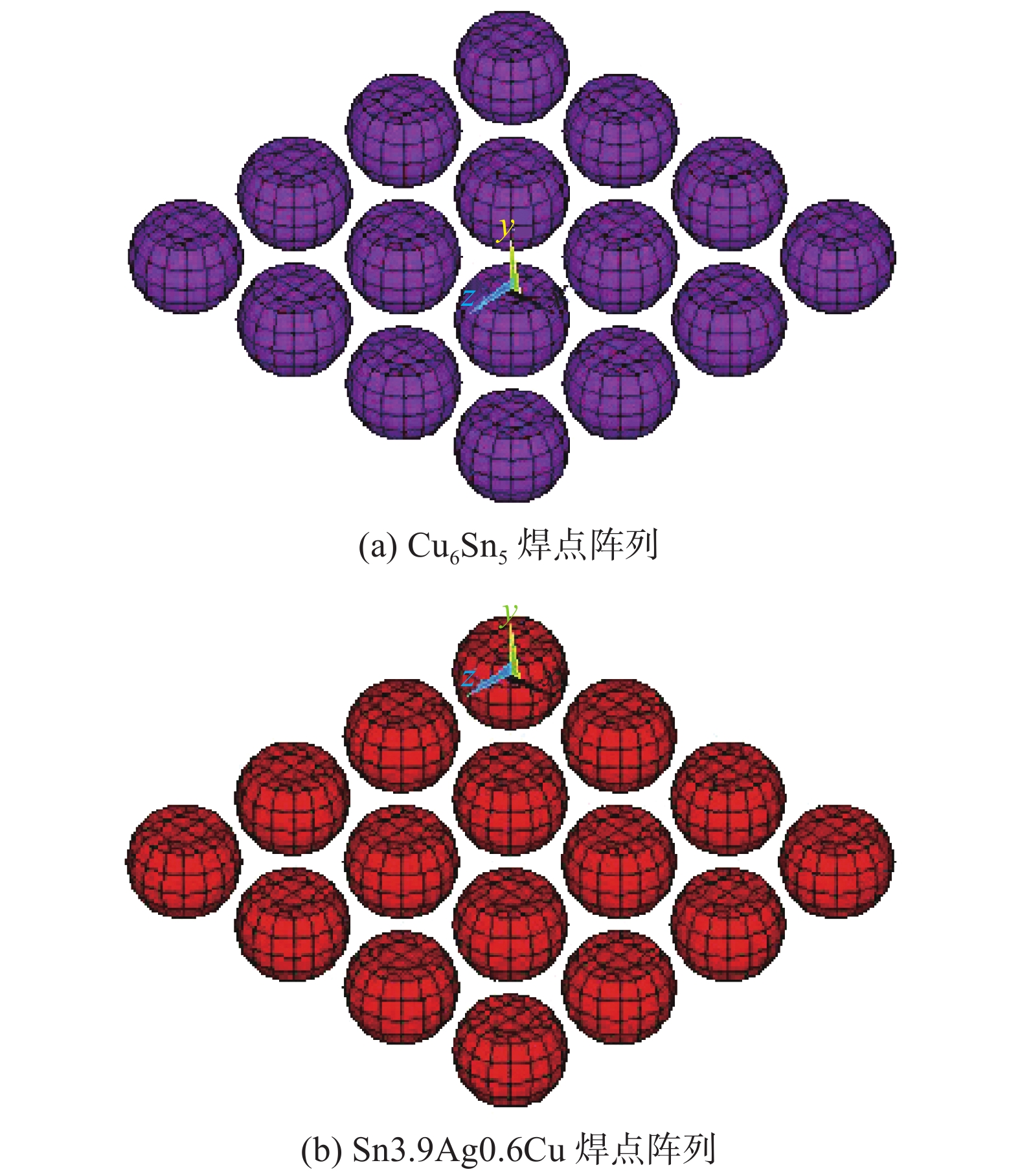
图 2 焊点阵列有限元模拟
Figure 2. Finite element model of solder joint. (a) Cu6Sn5; (b) Sn3.9Ag0.6Cu
表 1 材料参数
Table 1 Materials parameters
材料 弹性模量E/GPa 泊松比γ 热膨胀系数α/10−6K−1 屈服强度ReL/GPa 切变模量G/GPa 芯片 163 0.28 2.5 Cu柱 117 0.35 14.3 Cu6Sn5 124 0.30 19.0 1.86 50.4 Sn3.9Ag0.6Cu 74.84 0.30 16.6 BT基板 26 0.39 15.0  下载: 导出CSV
表 3 控制因子和水平
Table 3 Control factors and levels
控制因子 水平1 水平2 水平3 焊点材料A Sn3.9Ag0.6Cu Cu6Sn5 Cu3Sn 焊点阵列B 5 × 5 4 × 4 3 × 3 焊点高度C 0.08 mm 0.04 mm 0.02 mm 芯片厚度D 0.2 mm 0.1 mm 0.05 mm
下载: 导出CSV
表 4 田口正交试验方案
Table 4 Taguchi orthogonal test
试验 因子与水平 评价指标 S/N A B C D Δσ/GPa 1 1 1 1 1 0.055 8 25.07 2 1 2 2 2 0.047 5 26.47 3 1 3 3 3 0.041 0 27.74 4 2 1 2 3 0.056 2 25.00 5 2 2 3 1 0.044 7 26.99 6 2 3 1 2 0.015 9 27.33 7 3 1 3 2 0.057 1 24.87 8 3 2 1 3 0.051 4 25.78 9 3 3 2 1 0.017 8 27.70 平均值 26.33
下载: 导出CSV
表 5 信噪比S/N平均效应响应
Table 5 Average effect response for S/N ratio
水平 A B C D 水平1 26.43 24.98 26.06 26.59 水平2 26.44 26.41 26.39 26.22 水平3 26.11 27.59 26.53 26.17 效应 0.33 2.61 0.47 0.42 排名 4 1 2 3
下载: 导出CSV
-
[1] Sun L, Chen M H, Zhang L, et al. Recent progress in SLID bonding in novel 3D-IC technologies[J]. Journal of Alloys and Compounds, 2020, 818: 152825. doi: 10.1016/j.jallcom.2019.152825
[2] Hang C J, Tian Y H, Zhang R, et al. Phase transformation and grain orientation of Cu-Sn intermetallic compounds during low temperature bonding process[J]. Journal of Materials Science: Materials in Electronics, 2013, 24(10): 3905 − 3913. doi: 10.1007/s10854-013-1337-5
[3] 吕亚平, 刘孝刚, 陈明祥, 等. 含TSV结构的3D封装多层堆叠Cu/Sn键合技术[J]. 先进封装技术, 2014, 39(1): 64 − 70. Lü Yaping, Liu Xiaogang, Chen Mingxiang, et al. Multilayer stack Cu/Sn bonding technology for 3D packaging with TSV[J]. Advanced Packaging Technologies, 2014, 39(1): 64 − 70.
[4] 张亮, 韩继光, 郭永环, 等. WLCSP器件Sn3.9Ag0.6Cu焊点疲劳寿命预测[J]. 焊接学报, 2012, 33(3): 97 − 100. Zhang Liang, Han Jiguang, Guo Yonghuan, et al. Fatigue life prediction of Sn3.9Ag0.6Cu-soldered joints in WLCSP device[J]. Transactions of the China Welding Institution, 2012, 33(3): 97 − 100.
[5] 田艳红, 王宁, 杨东升, 等. 三维封装芯片键合IMC焊点应力分析及结构优化[J]. 焊接学报, 2012, 33(8): 17 − 20. Tian Yanhong, Wang Ning, Yang Dongsheng, et al. Stress analysis and structure optimization of IMC joints in 3D package[J]. Transactions of the China Welding Institution, 2012, 33(8): 17 − 20.
[6] 邵良滨, 黄春跃, 梁颖, 等. 基于热-结构耦合的叠层金凸点应力分析[J]. 焊接学报, 2017, 38(1): 31 − 34. Shao Liangbin, Huang Chunyue, Liang Ying, et al. Study on stacked AU bumps stress based on thermal-structure coupling[J]. Transactions of the China Welding Institution, 2017, 38(1): 31 − 34.
[7] 陈照辉. 大功率LED封装和硅通孔三维封装工艺及可靠性数值仿真与试验研究[D]. 上海: 上海交通大学, 2012. Chen Zhaohui. Study on process and reliability of high power LED packaging and through silicon via 3D packaging by simulation and experiment[D]. Shanghai: Shanghai Jiao Tong University, 2012.
[8] 韩立帅, 黄春跃, 梁颖, 等. 3D封装微尺度CSP焊点随机振动应力应变分析[J]. 焊接学报, 2019, 40(6): 64 − 70. doi: 10.12073/j.hjxb.2019400156 Han Lishuai, Huang Chunyue, Liang Ying, et al. Analysis of stress strain and shape size optimization of 3D micro-scale CSP solder joints in random vibration[J]. Transactions of the China Welding Institution, 2019, 40(6): 64 − 70. doi: 10.12073/j.hjxb.2019400156
[9] Annuar S, Mahmoodian R, Hamdi M, et al. Intermetallic compounds in 3D integrated circuits technology: a brief review[J]. Science and Technology of Advanced Materials, 2017, 18(1): 693 − 703. doi: 10.1080/14686996.2017.1364975
[10] Lall P, Islam M N, Singh N, et al. Model for BGA and CSP reliability in automotive underhood applications[J]. IEEE Transactions on Components and Packaging Technologies, 2004, 27(3): 585 − 593. doi: 10.1109/TCAPT.2004.831824
[11] 梁颖, 黄春跃, 黄伟, 等. 基于正交设计的WLCSP柔性无铅焊点随机激励应力应变分析[J]. 焊接学报, 2016, 37(2): 13 − 16. Liang Ying, Huang Chunyue, Huang Wei, et al. Stress and strain distribution of lead-free solder joints with compliant layer in wafer level chip scale package under random vibration based on orthogonal design[J]. Transactions of the China Welding Institution, 2016, 37(2): 13 − 16.
[12] 胡丹, 沈骏, 陈旭, 等. 正弦振动引起的BGA焊点Sn-Cu金属间化合物失效机理[J]. 中国有色金属学报, 2019, 29(4): 756 − 763. Hu Dan, Shen Jun, Chen Xu, et al. Fracture mechanism of Sn-Cu intermetallic compound layer in BGA solder joint induced by sinusoidal vibration[J]. The Chinese Journal of Nonferrous Metals, 2019, 29(4): 756 − 763.
[13] 张亮, 韩继光, 郭永环, 等. WLCSP器件结构优化模拟及无铅焊点可靠性[J]. 焊接学报, 2012, 33(7): 53 − 56. Zhang Liang, Han Jiguang, Guo Yonghuan, et al. Optimum simulation and soldered joints reliability of WLCSP device[J]. Transactions of the China Welding Institution, 2012, 33(7): 53 − 56.
[14] Zhang L, Han J G, Guo Y H, et al. Anand model and FEM analysis of SnAgCuZn lead-free solder joints in Wafer Level Chip Scale Packaging devices[J]. Microelectronics Reliability, 2014, 54(1): 281 − 286. doi: 10.1016/j.microrel.2013.07.100
[15] Samavatian M, Samavation V, Moayeri M, et al. Effect of stress triaxiality on damage evolution of porous solder joints in IGBT discretes[J]. Journal of Manufacturing Processes, 2018, 32: 57 − 64. doi: 10.1016/j.jmapro.2018.01.025
[16] Wu K C, Lin S Y, Hung T Y, et al. Reliability assessment of packaging solder joints under different thermal cycle loading rates[J]. IEEE Transactions on Device and Materials Reliability, 2015, 15(3): 437 − 442. doi: 10.1109/TDMR.2015.2462726
[17] Zhang L, Sun L, Guo Y H, et al. Reliability of lead-free solder joints in CSP device under thermal cycling[J]. Journal of Materials Science: Materials in Electronics, 2014, 25: 1209 − 1213. doi: 10.1007/s10854-014-1711-y
[18] Ladani L J. Stress analysis of 3-dimensional IC package as function of structural design parameters[J]. Microelectronic Engineering, 2010, 87(10): 1852 − 1860. doi: 10.1016/j.mee.2009.11.002
[19] Li M H C, Hong S M. Optimal parameter design for chip-on-film technology using the Taguchi method[J]. The International Journal of Advanced Manufacturing Technology, 2005, 25(1−2): 145 − 153. doi: 10.1007/s00170-003-1824-6
[20] Tsai T N, Liukkonen M. Robust parameter design for the micro-BGA stencil printing process using a fuzzy logic-based Taguchi method[J]. Applied Soft Computing, 2016, 48: 124 − 136. doi: 10.1016/j.asoc.2016.06.020
[21] Mertol A. Application of the Taguchi method on the robust design of molded 225 plastic ball grid array packages[J]. IEEE Transactions on Components, Packaging, and Manufacturing Technology, 1995, 18(4): 734 − 743. doi: 10.1109/96.475283


计量
- 文章访问数: 800
- HTML全文浏览量: 84
- PDF下载量: 91
